KFM4GH6Q4M KFN8GH6Q4M KFKAGH6Q4M
Remark
Initial issue
Revision No History Draft Date
Corrected errata
Oct
Ordering Information
General Overview
Device Performance
Product Features
Device Architecture
System Hardware
Detailed Product Description
Definitions
Pin Configuration
1 4Gb KFM4GH6Q4M / 8Gb KFN8GH6Q4M
63ball, 10mm x 13mm x max 1.0mmt , 0.8mm ball pitch FBGA4Gb
2 16Gb Product KFKAGH6Q4M TBD
TOP VIEW, Balls Facing Down 63ball Fbga OneNAND Chip
Register read cycles
Pin Description
Multiplexed Address/Data bus
Interrupt
Internal Nand Array Memory Organization
Block Diagram
Memory Array Organization
OTP
Sector
BlockMLC
BlockSLC
External BufferRAM Memory
BootRAM 1KB DataRAM0 2KB DataRAM1 2KB
Boot code Nand Array OTP Block
Internal Nand Array Memory
0000h
Memory Map
Block Block Address Size
256KB
Block Block Address
Block129
Block128
Block160
Block161
Block238 00EEh
Block240 00F0h
Block289 0121h Block258
Block256
Block288 0120h Block257
Block290 0122h Block259
Block353 0161h Block322
Block320
Block352 0160h Block321
Block354 0162h Block323
Block385
Block384
Block416
Block417
Block494 01EEh
Block496 01F0h
Block545 0221h Block514
Block512
Block544 0220h Block513
Block546 0222h Block515
Block609 0261h Block578
Block576
Block608 0260h Block577
Block610 0262h Block579
Block641
Block640
Block672
Block673
Block750 02EEh
Block752 02F0h
Block801 0321h Block770
Block768
Block800 0320h Block769
Block802 0322h Block771
Block865 0361h Block834
Block832
Block864 0360h Block833
Block866 0362h Block835
Block897
Block896
Block928
Block929
Block1006 03EEh
Block1008 03F0h
256W
Internal Memory Spare Area Assignment
Area
Byte
External Memory BufferRAM Address Map
Division Address Size Usage Description
External Memory Map Detail Information
BootRAMMain area
BootRAMSpare area
DataRAMMain area
External Memory Spare Area Assignment
Buf Word Byte
10054h 802Bh 10056h 802Ch 10058h 802Dh
10074h 803Bh 10076h 803Ch 10078h 803Dh
4bit ECC parity values 8046h 1008Ch 8047h 1008Eh
10092h Managed by internal ECC logic
DataS
10090h BIBad block Information
10094h 804Bh 10096h 804Ch 10098h 804Dh
Registers
Register Address Map
Address Name Host Description
Device ID Register F001h R
Device ID Default
Manufacturer ID Register F000h R
Device Identification
Version ID Register F002h
Data Buffer Size Register F003h R
This register is reserved for future use
Boot Buffer Size Register F004h R
Amount of Buffers Register F005h R
Technology Register F006h R
Start Address1 Register F100h R/W
Start Address2 Register F101h R/W
11~15 Start Address3~7 Register F102h~F106h
Start Address8 Register F107h R/W
Start Buffer Register F200h R/W
Sector allocation according to BSCCASE2 FSA=01 BSC =
Sector allocation according to BSCCASE1 FSA=00 BSC =
BSC =111
Sector allocation according to BSCCASE3 FSA=10 BSC =
CMD
Command Register F220h R/W
Acceptable
Operation
Two Methods to Clear Interrupt Register in Command Input
Write command into INT will automatically
Interrupt Register
System Configuration 1 Register F221h R, R/W
Brwl
Burst Length BL Information119
Burst Length BL
Burst LengthMain Burst LengthSpare
RDY Polarity RDYpol Information7
Iobe
MRSMode Register Setting Description
Write Mode WM
Write Mode Information1 Definition Description
Bwps
PIL
System Configuration 2 Register F222h
Controller Status Register F240h R
Otpl Otpbl
Otpl
Interrupt Status Register F241h R/W
INT
Rsti
Read Interrupt RI
WI Interrupt Status Conditions Default State Valid
EI Interrupt Status Conditions Default State Valid
RI Interrupt Status Conditions
Nand Flash Write Protection Status Register F24Eh R
Start Block Address Register F24Ch R/W
Start Block Address Register F24Dh R/W
SBA
ECC Status Register 4 FF03h R FF03h, default = 0000h
ECC Status Register 2 FF01h R FF01h, default = 0000h
ECC Status Register 3 FF02h R FF02h, default = 0000h
ECC Status Register 1 FF00h R
Command Based Operation
Reset Flex-MuxOneNAND Add BP1 Data 00F0h
Add Data 00E0h 0000h3 Read Identification Data XXXXh4 0090h
Read Identification Data Command
Reset Flex-MuxOneNAND Command
Load Data Into Buffer Command
Identification Data Description Address Data Out
Device Bus Operation
Operation ADQ0~15
CLK AVD
Reset Mode Operation
BP-F0h
Hot Reset Mode Operation
Cold Reset Mode Operation
Warm Reset Mode Operation
Nand Flash Core Reset Mode Operation
Nand Flash Array Write Protection Operation
BootRAM Write Protection Operation
Write Protection Operation
Nand Array Write Protection States
Locked Lock Command Sequence
Unlocked Unlock Command Sequence
Unlocked All Block Unlock Command Sequence
Unlocked Nand Array Write Protection State
Start block address+Lock-tight block command 002Ch
Nand Flash Array Write Protection State Diagram
Locked-tight Lock-Tight Command Sequence
Locked-tight Nand Array Write Protection State
DBS, DFS is for DDP
Samsung strongly recommends to follow the above flow chart
Lock/Unlock/Lock-TightError completed
DQ10=0?
All Block Unlock Completed
Data Protection During Power Down Operation
Load Operation
Superload Operation
LSB Page Recovery Read
Asynchronous Read Mode Operation RM=0, WM=0
Synchronous Read Mode Operation RM=1, WM=X
Read Operation
Continuous Linear Burst Read Operation
2.2 4-, 8-, 16-, 32-Word Linear Burst Read Operation
Reserved area is not available on Synchronous read
Output Disable Mode Operation
Programmable Burst Read Latency Operation
Handshaking Operation
See Timing Diagram 6.6, 6.7
Synchronous WriteRM=1, WM=1
Data register
Program Operation
Addressing for program operation
MLC Block
Paired Page Address Information
Paired Page Address
Flash Memory
If program operation results in an error, map out
Block including the page in error and copy
DBS, DFS is for DDP Target data to another block
Program Interleave can work in Auto INT
Interrupt register must not be written
DBS, DFS is for DDP
Cache Program Operation
Sector0 Sector7
Last PGM?
Cache Program Operation Flow Diagram
Program Error
Add F101h DQ=DBS Add DataRAM DQ=Data4KB
Interleave Cache Program Operation
Results in an error
If program operation
Block
Add F241h DQ=0000h DQ=Data
Copy back completed Copy back Error
Copy-Back Program Operation with Random Data Input
Write ‘DFS , FBA’ o f Fla sh
Erase Error
Erase Operation
Block Erase Operation
Add F100h DQ=DFS*, FBA Add F101h DQ=DBS
Erase Interleave1 @DDP Flow Chart
INT=1Ready Erase Error
Add F101h DQ=DBS Add F241h DQ=5=EI
Erase Suspend / Erase Resume Operation
Erase Suspend During a Block Erase Operation
Erase Resume
Partition Information PI Block SLC Only
PI Block Boundary Information setting
PI Block Boundary Information setting steps
PI Block Boundary Information setting Flow Chart
PI Block Access mode entry
PI Block Access mode entry Flow Chart
PI Block Erase Operation Flow Chart In PI Block Access Mode
PI Block Erase
Erasing the PI Area
Programming the PI Area
PI Block Program Operation
Memory location in the PI area can be program
Locking the PI
PI Update
Update the PI Area
Add F241h DQ15=INT PI updated
PI Block Load Operation
OTP Operation SLC only
OTP Block Area Structure
1st Block OTP Area Structure
OTP Block Load Operation
OTP Exit
OTP Block Program Operation
Programming the OTP Area
Add DP DQ=Data-in
OTP Block Program Operation Flow Chart
Do Cold/Warm/Hot Nand Flash Core reset OTP Exit
OTPL=0? YES
OTP Block Lock Operation
Locking the OTP
OTP Lock Operation Steps
Add F241h DQ15=INT Do Cold reset
Automatically Updated
Add F241h DQ15=INT Write Data into DataRAM3 Add 1st Word
13.4 1st Block OTP Lock Operation
Locking the 1st Block OTP
1st Block OTP Lock Operation Steps
100
OTP and 1st Block OTP Lock Operation
Locking the OTP and 1st Block OTP
OTP and 1st Block OTP simultaneous Lock Operation Steps
102
DQ6 DQ5~DQ0
14 DQ6 Toggle Bit
Status DQ15~DQ7
Progress Data Loading Don’t Care
ECC Operation
ECC Bypass Operation
Invalid Block Operation
Invalid Block Identification Table Operation
Invalid Block Replacement Operation
Invalid Block Table Creation Flow Chart Start
1st 1th Nth
Block Replacement Operation Sequence
Block a
1st Block B 1th Nth 107
Absolute Maximum Ratings
Operating Conditions
KFM4GH6Q4M
DC Characteristics
Parameter
Test Conditions
Device Capacitance
Valid Block Characteristics
AC Test Conditions
DDP QDP
66MHz 83MHz Unit
AC Characteristics for Synchronous Burst Read
See Timing Diagrams 6.1 Parameter
Max Min
KFKAGH6Q4MTBD
AC Characteristics for Asynchronous Read
KFN8GH6Q4M
Min Max
AC Characteristics for Asynchronous Write
AC Characteristics for Burst Write Operation
See Timing Diagrams Parameter Symbol Min Max Unit
200
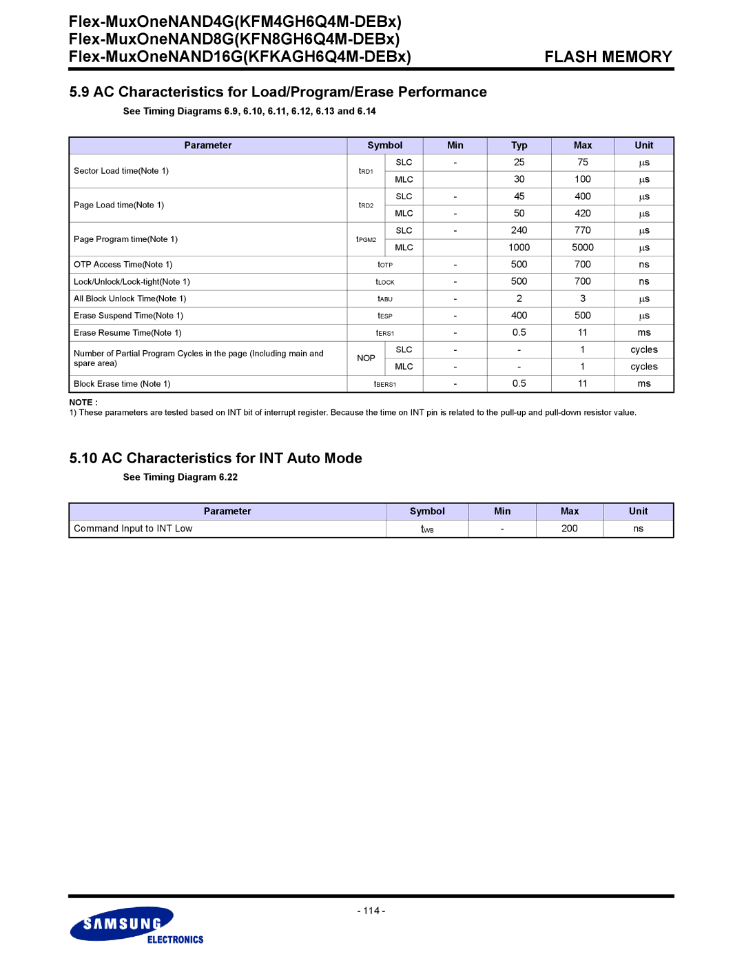
AC Characteristics for Load/Program/Erase Performance
AC Characteristics for INT Auto Mode
114
CLK
8-Word Linear Burst Read Mode with Wrap Around
Continuous Linear Burst Read Mode with Wrap Around
RDY
Low
See AC Characteristics Table DQ0 DQ15
Asynchronous Read VA Transition Before
Asynchronous Read VA Transition After AVD Low
Valid WD
Asynchronous Write
ADQ15-ADQ0
Hi-Z
≈D7
8-Word Linear Burst Write Mode
Burst Write Operation followed by Burst Read
118
Start Initial Burst Write Operation
119
Load Operation Timing
See AC Characteristics .7 and Table
Load Command Sequence last two cycles Read Data
Completed Da+n
Superload Operation Timing
Program Command Sequence last two cycles
Program Operation Timing
122
Timing
Ongoing Status
ADQ15
Interleave Cache Program Operation
ADQ0~
Ongoing Status INT bit
Erase Command Sequence
Block Erase Operation Timing
125
Cold Reset Timing
Warm Reset Timing
CE, OE
127
Hot Reset Timing
Flex-MuxOneNAND
ADQi
Flex-MuxOneNAND Operation or Idle Nand Flash Core reset
Nand Flash Core Reset Timing
Data Protection Timing During Power Down
ADQi
Status RD Hi-Z
RDY
130
INT auto mode
Write command into Command Register INT will automatically
131
General Operation DQ type
Methods of Determining Interrupt Status
INT Type Mono INT Type DDP
132
Synchronous Mode Using the INT Pin
Asynchronous Mode Using the INT Pin
INT Pin to a Host General Purpose I/O
Polling the Interrupt Register Status Bit
134
INT pol = ‘High’ Default
Determining Rp Value DDP, QDP Only
Rpohm
Ready
INT pol = ‘Low’
Vcc or Vccq
Vss KFN8GH6Q4M @ Vcc = 1.8V, Ta = 25C , CL = 30pF
Boot Sequence
Boot Sequence
Boot Loaders in Flex-MuxOneNAND
Boot Loaders in Flex-MuxOneNAND Description
BL1
NBL3
BL2
NBL2
Last Block Address First Block Address
Partition of Flex-MuxOneNAND
MLC Partition +1 ~ n-1 Blocks
Data Register
DDP and QDP Description
DDPDual Die Package
QDPQuad Die Package
4G product KFM4GH6Q4M
8G product KFN8GH6Q4M
141
16G product KFKAGH6Q4M
142