CY7B9911V 3.3V RoboClock+™
groups, and the PLL aligns the rising edges of REF and FB, you can create wider output skews by proper selection of the xFn inputs. For example, a +10 tU between REF and 3Qx is achieved by connecting 1Q0 to FB and setting 1F0 = 1F1 = GND, 3F0 = MID, and 3F1 = High. (Since FB aligns at
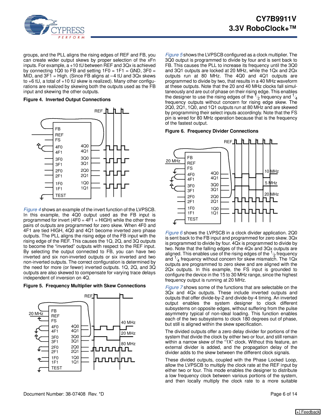
Figure 4. Inverted Output Connections
| REF |
FB |
|
REF |
|
FS |
|
4F0 | 4Q0 |
4F1 | 4Q1 |
3F0 | 3Q0 |
3F1 | 3Q1 |
2F0 | 2Q0 |
2F1 | 2Q1 |
1F0 | 1Q0 |
1F1 | 1Q1 |
TEST |
|
Figure 4 shows an example of the invert function of the LVPSCB. In this example, the 4Q0 output used as the FB input is programmed for invert (4F0 = 4F1 = HIGH) while the other three pairs of outputs are programmed for zero skew. When 4F0 and 4F1 are tied HIGH, 4Q0 and 4Q1 become inverted zero phase outputs. The PLL aligns the rising edge of the FB input with the rising edge of the REF. This causes the 1Q, 2Q, and 3Q outputs to become the “inverted” outputs with respect to the REF input. By selecting the output connected to FB, you can have two inverted and six non-inverted outputs or six inverted and two non-inverted outputs. The correct configuration is determined by the need for more (or fewer) inverted outputs. 1Q, 2Q, and 3Q outputs are also skewed to compensate for varying trace delays independent of inversion on 4Q.
Figure 5. Frequency Multiplier with Skew Connections
|
|
| REF |
20 MHz | FB |
|
|
REF |
|
| |
|
|
| |
| FS |
| 40 MHz |
| 4F0 | 4Q0 | |
|
| ||
| 4F1 | 4Q1 | 20 MHz |
| 3F0 | 3Q0 | |
|
| ||
| 3F1 | 3Q1 | 80 MHz |
| 2F0 | 2Q0 | |
|
| ||
| 2F1 | 2Q1 |
|
| 1F0 | 1Q0 |
|
| 1F1 | 1Q1 |
|
| TEST |
|
|
Figure 5 shows the LVPSCB configured as a clock multiplier. The 3Q0 output is programmed to divide by four and is sent back to FB. This causes the PLL to increase its frequency until the 3Q0 and 3Q1 outputs are locked at 20 MHz, while the 1Qx and 2Qx outputs run at 80 MHz. The 4Q0 and 4Q1 outputs are programmed to divide by two, that results in a 40 MHz waveform at these outputs. Note that the 20 and 40 MHz clocks fall simul- taneously and are out of phase on their rising edge. This enables the designer to use the rising edges of the 1⁄2 frequency and 1⁄4 frequency outputs without concern for rising edge skew. The 2Q0, 2Q1, 1Q0, and 1Q1 outputs run at 80 MHz and are skewed by programming their select inputs accordingly. Note that the FS pin is wired for 80 MHz operation because that is the frequency of the fastest output.
Figure 6. Frequency Divider Connections
|
|
|
|
|
|
|
|
|
|
|
|
|
|
|
|
|
|
|
| REF |
|
|
|
|
|
|
|
|
|
|
|
|
| |||
|
|
|
|
|
|
|
|
|
|
|
|
|
|
|
|
|
|
|
|
|
|
|
|
|
|
|
|
|
|
|
|
|
|
|
|
|
|
|
|
|
|
|
|
|
|
|
|
|
|
|
|
|
|
|
|
|
|
|
|
|
|
|
|
|
|
|
|
|
|
|
|
|
|
|
|
|
|
|
|
|
|
|
|
|
|
|
|
|
|
|
|
|
|
|
|
|
|
|
|
|
|
|
|
|
|
|
| |||
|
|
|
|
|
|
|
|
|
| FB |
|
|
|
|
|
|
|
|
|
|
|
|
|
|
|
|
|
|
|
|
|
|
| |||
20 MHz |
|
|
|
|
|
|
|
|
|
|
|
|
|
|
|
|
|
|
|
|
|
|
| |||||||||||||
REF |
|
|
|
|
|
|
|
|
|
|
|
|
|
|
|
|
|
|
|
|
|
|
| |||||||||||||
|
|
|
|
|
|
|
|
|
|
|
|
|
|
|
|
|
|
|
|
|
|
|
|
|
|
|
|
|
|
|
|
| ||||
|
|
|
|
|
|
|
|
|
| FS |
| 4Q0 |
|
|
|
|
|
|
|
|
|
|
|
|
| 10 MHz | ||||||||||
|
|
|
|
|
|
|
|
|
|
|
|
|
|
|
|
|
|
|
|
|
|
|
| |||||||||||||
|
|
|
|
|
|
|
|
|
| 4F0 |
|
|
|
|
|
|
|
|
|
|
|
|
|
| ||||||||||||
|
|
|
|
|
|
|
|
|
|
|
|
|
|
|
|
|
|
|
|
|
|
|
|
|
|
|
|
| ||||||||
|
|
|
|
|
|
|
|
|
| 4F1 |
| 4Q1 |
|
|
|
|
|
|
|
|
|
|
|
|
|
|
|
|
|
| ||||||
|
|
|
|
|
|
|
|
|
| 3F0 |
| 3Q0 |
|
|
|
|
|
|
|
|
|
|
|
|
| 5 MHz | ||||||||||
|
|
|
|
|
|
|
|
|
|
|
|
|
|
|
|
|
|
|
|
|
|
|
|
|
|
|
|
| ||||||||
|
|
|
|
|
|
|
|
|
| 3F1 |
| 3Q1 |
|
|
|
|
|
|
|
|
|
|
|
|
| 20 MHz | ||||||||||
|
|
|
|
|
|
|
|
|
|
|
|
|
|
|
|
|
|
|
|
|
|
|
| |||||||||||||
|
|
|
|
|
|
|
|
|
|
|
|
|
|
|
|
|
|
|
|
|
|
| ||||||||||||||
|
|
|
|
|
|
|
|
|
| 2F0 |
| 2Q0 |
|
|
|
|
|
|
|
|
|
|
|
|
| |||||||||||
|
|
|
|
|
|
|
|
|
| 2F1 |
| 2Q1 |
|
|
|
|
|
|
|
|
|
|
|
|
|
|
|
|
|
| ||||||
|
|
|
|
|
|
|
|
|
|
|
|
|
|
|
|
|
|
|
|
|
|
|
|
|
|
|
| |||||||||
1F0 1Q0
1F1 1Q1 ![]()
![]()
![]() TEST
TEST
Figure 6 shows the LVPSCB in a clock divider application. 2Q0 is sent back to the FB input and programmed for zero skew. 3Qx is programmed to divide by four. 4Qx is programmed to divide by two. Note that the falling edges of the 4Qx and 3Qx outputs are aligned. This enables use of the rising edges of the 1⁄2 frequency and 1⁄4 frequency without concern for skew mismatch. The 1Qx outputs are programmed to zero skew and are aligned with the 2Qx outputs. In this example, the FS input is grounded to configure the device in the 15 to 30 MHz range, since the highest frequency output is running at 20 MHz.
Figure 7 shows some of the functions that are selectable on the 3Qx and 4Qx outputs. These include inverted outputs and outputs that offer divide-by-2 and divide-by-4 timing. An inverted output enables the system designer to clock different subsystems on opposite edges, without suffering from the pulse asymmetry typical of non-ideal loading. This function enables each of the two subsystems to clock 180 degrees out of phase, but still is aligned within the skew specification.
The divided outputs offer a zero delay divider for portions of the system that divide the clock by either two or four, and still remain within a narrow skew of the “1X” clock. Without this feature, an external divider is added, and the propagation delay of the divider adds to the skew between the different clock signals.
These divided outputs, coupled with the Phase Locked Loop, allow the LVPSCB to multiply the clock rate at the REF input by either two or four. This mode enables the designer to distribute a low frequency clock between various portions of the system, and then locally multiply the clock rate to a more suitable
Document Number: | Page 6 of 14 |
[+] Feedback