CY7B9911V 3.3V RoboClock+™
Capacitance
Tested initially and after any design or process changes that may affect these parameters.[10]
Parameter | Description | Test Conditions | Max | Unit |
CIN | Input Capacitance | TA = 25°C, f = 1 MHz, VCC = 3.3V | 10 | pF |
Note
10. Applies to REF and FB inputs only.
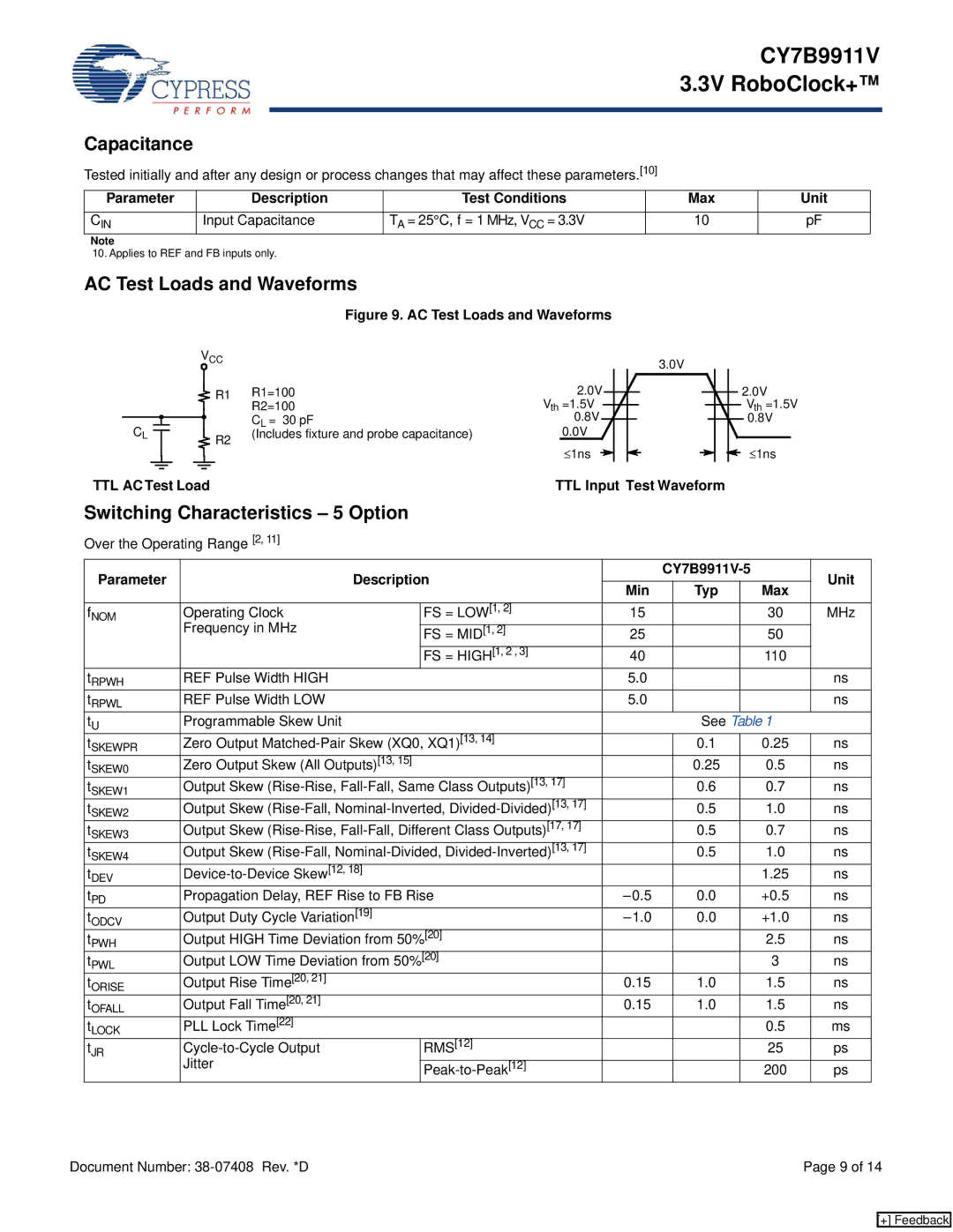
AC Test Loads and Waveforms
Figure 9. AC Test Loads and Waveforms
| VCC |
| 3.0V |
|
|
| |
| R1 | R1=100 | 2.0V |
|
| R2=100 | Vth =1.5V |
CL |
| CL = 30 pF | 0.8V |
R2 | (Includes fixture and probe capacitance) | 0.0V | |
|
| ≤1ns | |
|
|
|
2.0V
Vth =1.5V 0.8V
≤1ns
TTL ACTest Load |
| TTL Input Test Waveform |
|
| |||||
Switching Characteristics – 5 Option |
|
|
|
|
|
|
|
| |
Over the Operating Range [2, 11] |
|
|
|
|
|
|
|
| |
Parameter | Description |
|
|
| Unit | ||||
|
|
|
|
|
| ||||
| Min |
| Typ |
| Max | ||||
|
|
|
|
|
|
| |||
fNOM | Operating Clock | FS = LOW[1, 2] |
| 15 |
|
|
| 30 | MHz |
| Frequency in MHz |
|
|
|
|
|
|
|
|
| FS = MID[1, 2] |
| 25 |
|
|
| 50 |
| |
|
| FS = HIGH[1, 2 , 3] |
| 40 |
|
|
| 110 |
|
tRPWH | REF Pulse Width HIGH |
|
| 5.0 |
|
|
|
| ns |
tRPWL | REF Pulse Width LOW |
|
| 5.0 |
|
|
|
| ns |
tU | Programmable Skew Unit |
|
|
|
| See Table 1 |
| ||
tSKEWPR | Zero Output |
|
|
| 0.1 |
| 0.25 | ns | |
tSKEW0 | Zero Output Skew (All Outputs)[13, 15] |
|
|
|
| 0.25 |
| 0.5 | ns |
tSKEW1 | Output Skew |
|
| 0.6 |
| 0.7 | ns | ||
tSKEW2 | Output Skew |
|
| 0.5 |
| 1.0 | ns | ||
tSKEW3 | Output Skew |
|
| 0.5 |
| 0.7 | ns | ||
tSKEW4 | Output Skew |
|
| 0.5 |
| 1.0 | ns | ||
tDEV |
|
|
|
|
|
| 1.25 | ns | |
tPD | Propagation Delay, REF Rise to FB Rise |
|
| 0.0 |
| +0.5 | ns | ||
tODCV | Output Duty Cycle Variation[19] |
|
|
| 0.0 |
| +1.0 | ns | |
tPWH | Output HIGH Time Deviation from 50%[20] |
|
|
|
|
| 2.5 | ns | |
tPWL | Output LOW Time Deviation from 50%[20] |
|
|
|
|
| 3 | ns | |
tORISE | Output Rise Time[20, 21] |
|
| 0.15 |
| 1.0 |
| 1.5 | ns |
tOFALL | Output Fall Time[20, 21] |
|
| 0.15 |
| 1.0 |
| 1.5 | ns |
tLOCK | PLL Lock Time[22] |
|
|
|
|
|
| 0.5 | ms |
tJR | RMS[12] |
|
|
|
|
| 25 | ps | |
| Jitter |
|
|
|
|
|
|
|
|
|
|
|
|
|
| 200 | ps | ||
Document Number: | Page 9 of 14 |
[+] Feedback