Features
■High speed
❐tAA = 10 ns
■Low active power
❐ICC = 175 mA at 10 ns
■Low CMOS standby power
❐ISB2 = 25 mA
■Operating voltages of 3.3 ± 0.3V
■2.0V data retention
■Automatic power down when deselected
■TTL compatible inputs and outputs
■Available in
CY7C1012DV33
12-Mbit (512K X 24) Static RAM
Functional Description
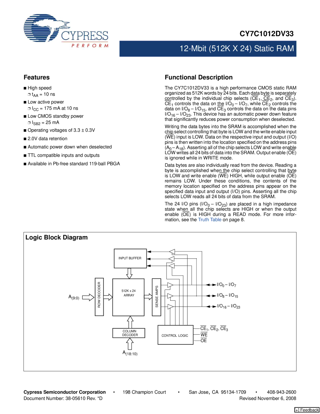
The CY7C1012DV33 is a high performance CMOS static RAM organized as 512K words by 24 bits. Each data byte is separately controlled by the individual chip selects (CE1, CE2, and CE3). CE1 controls the data on the I/O0 – I/O7, while CE2 controls the data on I/O8 – I/O15, and CE3 controls the data on the data pins I/O16 – I/O23. This device has an automatic power down feature that significantly reduces power consumption when deselected.
Writing the data bytes into the SRAM is accomplished when the chip select controlling that byte is LOW and the write enable input (WE) input is LOW. Data on the respective input and output (I/O) pins is then written into the location specified on the address pins (A0 – A18). Asserting all of the chip selects LOW and write enable LOW writes all 24 bits of data into the SRAM. Output enable (OE) is ignored while in WRITE mode.
Data bytes are also individually read from the device. Reading a byte is accomplished when the chip select controlling that byte is LOW and write enable (WE) HIGH, while output enable (OE) remains LOW. Under these conditions, the contents of the memory location specified on the address pins appear on the specified data input and output (I/O) pins. Asserting all the chip selects LOW reads all 24 bits of data from the SRAM.
The 24 I/O pins (I/O0 – I/O23) are placed in a high impedance state when all the chip selects are HIGH or when the output enable (OE) is HIGH during a READ mode. For more infor- mation, see the Truth Table on page 8.
Logic Block Diagram
A(9:0)
ROW DECODER
INPUT BUFFER
512K x 24
ARRAY
COLUMN
DECODER
A(18:10)
SENSE AMPS |
CONTROL LOGIC
![]()
![]() I/O0 – I/O7
I/O0 – I/O7
![]()
![]() I/O8 – I/O15
I/O8 – I/O15
![]()
![]() I/O16 – I/O23
I/O16 – I/O23
CE1, CE2, CE3
WE
OE
Cypress Semiconductor Corporation • 198 Champion Court | • | San Jose, CA | • | |
Document Number: |
| Revised November 6, 2008 | ||
[+] Feedback