CY7C1012DV33
Capacitance
Tested initially and after any design or process changes that may affect these parameters.
Parameter | Description | Test Conditions | Max | Unit |
CIN | Input Capacitance | TA = 25°C, f = 1 MHz, VCC = 3.3V | 8 | pF |
COUT | I/O Capacitance |
| 10 | pF |
Thermal Resistance
Tested initially and after any design or process changes that may affect these parameters.
Parameter | Description |
| Test Conditions |
| Unit |
| PBGA | ||||
|
|
|
|
| |
ΘJA | Thermal Resistance |
| Still air, soldered on a 3 × 4.5 inch, | 20.31 | °C/W |
| (junction to ambient) |
| four layer printed circuit board |
|
|
ΘJC | Thermal Resistance |
|
| 8.35 | °C/W |
| (junction to case) |
|
|
|
|
|
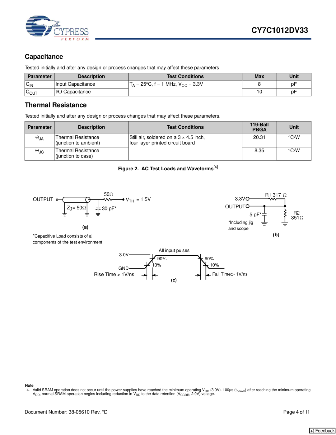
| Figure 2. AC Test Loads and Waveforms[4] |
|
| |
|
|
|
|
|
|
|
|
|
|
| 50Ω | ||
OUTPUT |
|
|
| Z0= 50Ω |
|
|
|
|
|
|
| VTH = 1.5V | |
|
|
|
|
|
|
|
|
| |||||
|
|
|
|
|
|
|
|
|
| ||||
|
|
|
|
|
|
|
| 30 pF* | |||||
|
|
|
|
|
|
|
| ||||||
|
|
|
|
|
|
|
| ||||||
|
|
|
|
|
|
|
|
|
|
|
|
|
|
|
|
|
|
|
|
|
|
|
|
|
|
|
|
|
|
|
|
|
|
|
|
|
|
|
|
|
|
|
|
|
| (a) |
|
|
|
|
|
|
| ||
3.3V | R1 317 Ω |
| |
OUTPUT | R2 |
5 pF* | |
| 351Ω |
*Including jig and scope
*Capacitive Load consists of all components of the test environment
3.0V
GND
Rise Time > 1V/ns
All input pulses
90%
10%
(c)
(b)
90%
10%
 Fall Time:> 1V/ns
Note
4.Valid SRAM operation does not occur until the power supplies have reached the minimum operating VDD (3.0V). 100μs (tpower) after reaching the minimum operating VDD, normal SRAM operation begins including reduction in VDD to the data retention (VCCDR, 2.0V) voltage.
Document Number: | Page 4 of 11 |
[+] Feedback