CY7C1217H specifications
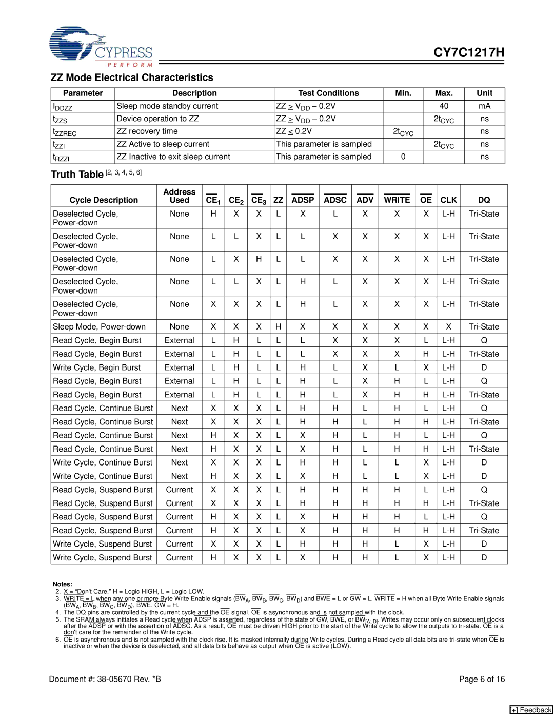
The Cypress CY7C1217H is a high-performance synchronous static random-access memory (SRAM) device that offers an array of features making it suitable for a diverse range of applications. With a configuration of 1 Meg x 16 bits, this component is well-suited for use in high-speed data processing systems, instrumentation, networking, and other applications that demand rapid-read and write cycles.One of the standout features of the CY7C1217H is its high-speed operation. It supports a clock frequency of up to 167 MHz, making it ideal for systems that require fast data access and transfer rates. This high-speed capability is complemented by a low-power consumption profile, which is critical for battery-operated devices and energy-efficient applications. The part operates on a supply voltage of 1.65V to 1.95V, allowing for compatibility with modern low-voltage digital systems.
The device utilizes a dual-port architecture, enabling simultaneous access from multiple processors or data buses. This dual-port design significantly improves performance by allowing multiple data transactions to occur simultaneously, thus increasing overall system throughput. Additionally, the CY7C1217H features an asynchronous read and write capability, allowing for flexible operation in various system configurations.
In terms of memory organization, the CY7C1217H employs a multiplexed address input design, which helps optimize pin count and leads to more efficient PCB layouts. The use of a XY address decoding scheme allows for straightforward integration into existing systems while maintaining high performance.
Another notable characteristic of this SRAM is its reliability and durability. The device is built using Cypress's advanced trench technology, providing inherent robustness against environmental stress factors. This ensures a longer lifespan and improved performance consistency over time.
Furthermore, the CY7C1217H supports a range of operating temperatures, making it suitable for both commercial and industrial applications. Whether used in consumer electronics or critical industrial control systems, this SRAM's versatility ensures it can meet diverse design requirements.
In summary, the Cypress CY7C1217H synchronous SRAM combines high-speed performance, low power consumption, and dual-port capabilities with robust design characteristics. Its versatility and reliability make it an excellent choice for engineers looking to enhance their high-performance applications across various sectors.

