|
|
|
|
|
|
|
|
|
|
|
|
|
| CY7C1266V18, CY7C1277V18 | |||
|
|
|
|
|
|
|
|
|
|
|
|
|
| CY7C1268V18, CY7C1270V18 | |||
|
|
|
|
|
|
|
|
|
|
|
|
|
|
|
| ||
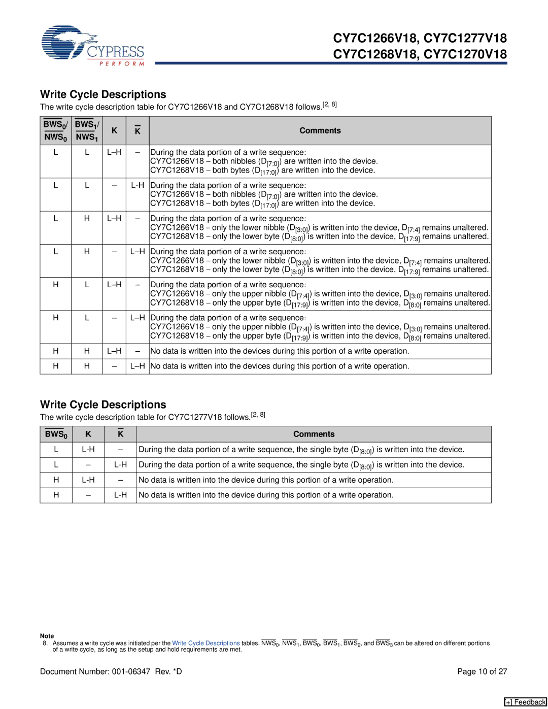
Write Cycle Descriptions |
|
|
| ||||||||||||||
The write cycle description table for CY7C1266V18 and CY7C1268V18 follows.[2, 8] |
|
|
| ||||||||||||||
| BWS | 0/ |
| BWS | 1/ | K |
|
|
|
|
|
| Comments |
|
|
| |
|
|
| K |
|
|
|
|
| |||||||||
|
|
|
|
|
|
|
|
|
|
|
|
| |||||
| NWS0 |
| NWS1 |
|
|
|
|
| |||||||||
|
|
|
|
|
|
|
|
|
|
|
|
|
| ||||
| L |
| L |
|
| – | During the data portion of a write sequence: |
|
|
| |||||||
|
|
|
|
|
|
|
|
|
|
|
| CY7C1266V18 − both nibbles (D[7:0]) are written into the device. |
|
|
| ||
|
|
|
|
|
|
|
|
|
|
|
| CY7C1268V18 − both bytes (D[17:0]) are written into the device. |
|
|
| ||
| L |
| L | – |
| During the data portion of a write sequence: |
|
|
| ||||||||
|
|
|
|
|
|
|
|
|
|
|
| CY7C1266V18 − both nibbles (D[7:0]) are written into the device. |
|
|
| ||
|
|
|
|
|
|
|
|
|
|
|
| CY7C1268V18 − both bytes (D[17:0]) are written into the device. |
|
|
| ||
| L |
| H |
|
| – | During the data portion of a write sequence: |
|
|
| |||||||
|
|
|
|
|
|
|
|
|
|
|
| CY7C1266V18 − only the lower nibble (D[3:0]) is written into the device, D[7:4] | remains unaltered. |
| |||
|
|
|
|
|
|
|
|
|
|
|
| CY7C1268V18 − only the lower byte (D[8:0]) is written into the device, D[17:9] | remains unaltered. |
| |||
| L |
| H | – |
| During the data portion of a write sequence: |
|
|
| ||||||||
|
|
|
|
|
|
|
|
|
|
|
| CY7C1266V18 − only the lower nibble (D[3:0]) is written into the device, D[7:4] | remains unaltered. |
| |||
|
|
|
|
|
|
|
|
|
|
|
| CY7C1268V18 − only the lower byte (D[8:0]) is written into the device, D[17:9] | remains unaltered. |
| |||
| H |
| L |
|
| – | During the data portion of a write sequence: |
|
|
| |||||||
|
|
|
|
|
|
|
|
|
|
|
| CY7C1266V18 − only the upper nibble (D[7:4]) is written into the device, D[3:0] | remains unaltered. |
| |||
|
|
|
|
|
|
|
|
|
|
|
| CY7C1268V18 − only the upper byte (D[17:9]) is written into the device, D[8:0] | remains unaltered. |
| |||
| H |
| L | – |
| During the data portion of a write sequence: |
|
|
| ||||||||
|
|
|
|
|
|
|
|
|
|
|
| CY7C1266V18 − only the upper nibble (D[7:4]) is written into the device, D[3:0] | remains unaltered. |
| |||
|
|
|
|
|
|
|
|
|
|
|
| CY7C1268V18 − only the upper byte (D[17:9]) is written into the device, D[8:0] | remains unaltered. |
| |||
| H |
| H |
|
| – | No data is written into the devices during this portion of a write operation. |
|
|
| |||||||
|
|
|
|
|
|
|
|
|
|
|
| ||||||
| H |
| H | – |
| No data is written into the devices during this portion of a write operation. |
|
|
| ||||||||
|
|
|
|
|
|
|
|
| |||||||||
Write Cycle Descriptions |
|
|
| ||||||||||||||
The write cycle description table for CY7C1277V18 follows.[2, 8] |
|
|
| ||||||||||||||
| BWS | 0 |
| K |
| K |
|
|
|
|
|
| Comments |
|
|
| |
| L |
|
| – |
| During the data portion of a write sequence, the single byte (D[8:0]) is written into the device. |
|
| |||||||||
| L |
| – |
| During the data portion of a write sequence, the single byte (D[8:0]) is written into the device. |
|
| ||||||||||
| H |
|
| – |
| No data is written into the device during this portion of a write operation. |
|
|
| ||||||||
|
|
|
|
|
|
|
|
|
| ||||||||
| H |
| – |
| No data is written into the device during this portion of a write operation. |
|
|
| |||||||||
|
|
|
|
|
|
|
|
|
|
|
|
|
|
|
|
|
|
Note
8.Assumes a write cycle was initiated per the Write Cycle Descriptions tables. NWS0, NWS1, BWS0, BWS1, BWS2, and BWS3 can be altered on different portions of a write cycle, as long as the setup and hold requirements are met.
Document Number: | Page 10 of 27 |
[+] Feedback