CY7C1266V18, CY7C1277V18
CY7C1268V18, CY7C1270V18
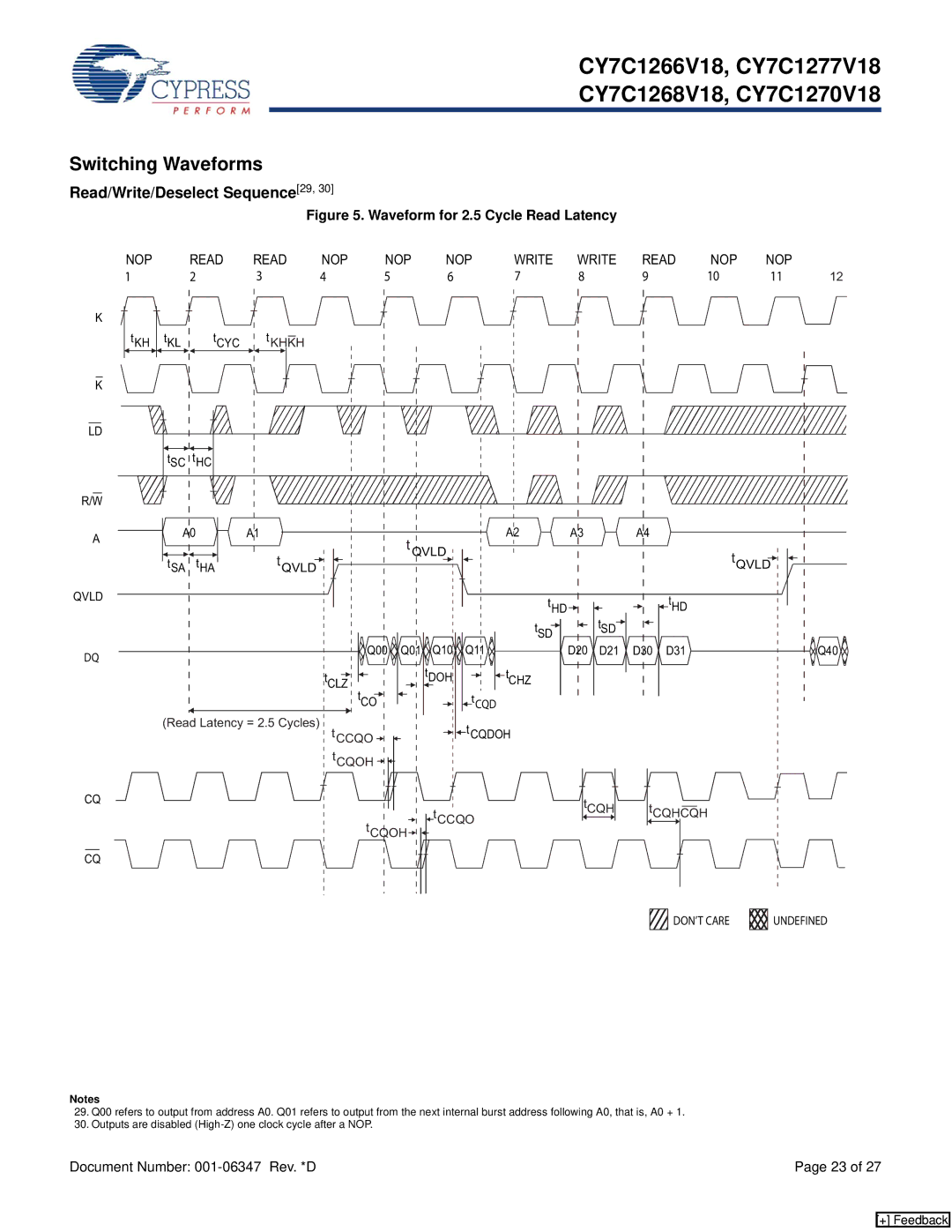
Switching Waveforms
Read/Write/Deselect Sequence[29, 30]
Figure 5. Waveform for 2.5 Cycle Read Latency
K
NOP
1
tKH
| READ | READ | NOP | NOP | NOP | WRITE | WRITE | READ | NOP | NOP |
|
| 2 | 3 | 4 | 5 | 6 | 7 | 8 | 9 | 10 | 11 | 12 |
tKL | tCYC | tKHKH |
|
|
|
|
|
|
|
|
|
K |
|
|
|
|
|
|
LD |
|
|
|
|
|
|
| tSC | tHC |
|
|
|
|
R/W |
|
|
|
|
|
|
A | A0 | A1 | A2 | A3 | A4 | |
|
|
| tQVLD |
|
| |
| tSA | tHA | tQVLD |
| tQVLD | |
|
|
| ||||
QVLD |
|
|
| tHD |
| tHD |
|
|
|
|
| tSD |
| ||
|
| Q01 Q10 | tSD |
|
| ||
DQ | Q00 | Q11 | D20 D21 | D30 D31 | Q40 | ||
| tDOH |
|
|
|
| ||
| tCLZ | tCHZ |
|
|
| ||
| tCO |
|
| tCQD |
|
|
|
| (Read Latency = 2.5 Cycles) |
|
| tCQDOH |
|
|
|
| tCCQO |
|
|
|
|
| |
| tCQOH |
|
|
|
|
|
|
CQ |
| t |
|
| tCQH | tCQHCQH |
|
|
| CCQO |
| ||||
| tCQOH |
|
|
| |||
|
|
|
|
|
| ||
CQ |
|
|
|
|
|
|
|
|
|
|
|
|
| DON’T CARE | UNDEFINED |
Notes
29.Q00 refers to output from address A0. Q01 refers to output from the next internal burst address following A0, that is, A0 + 1.
30.Outputs are disabled
Document Number: | Page 23 of 27 |
[+] Feedback