CY7C132, CY7C136
CY7C136A, CY7C142, CY7C146
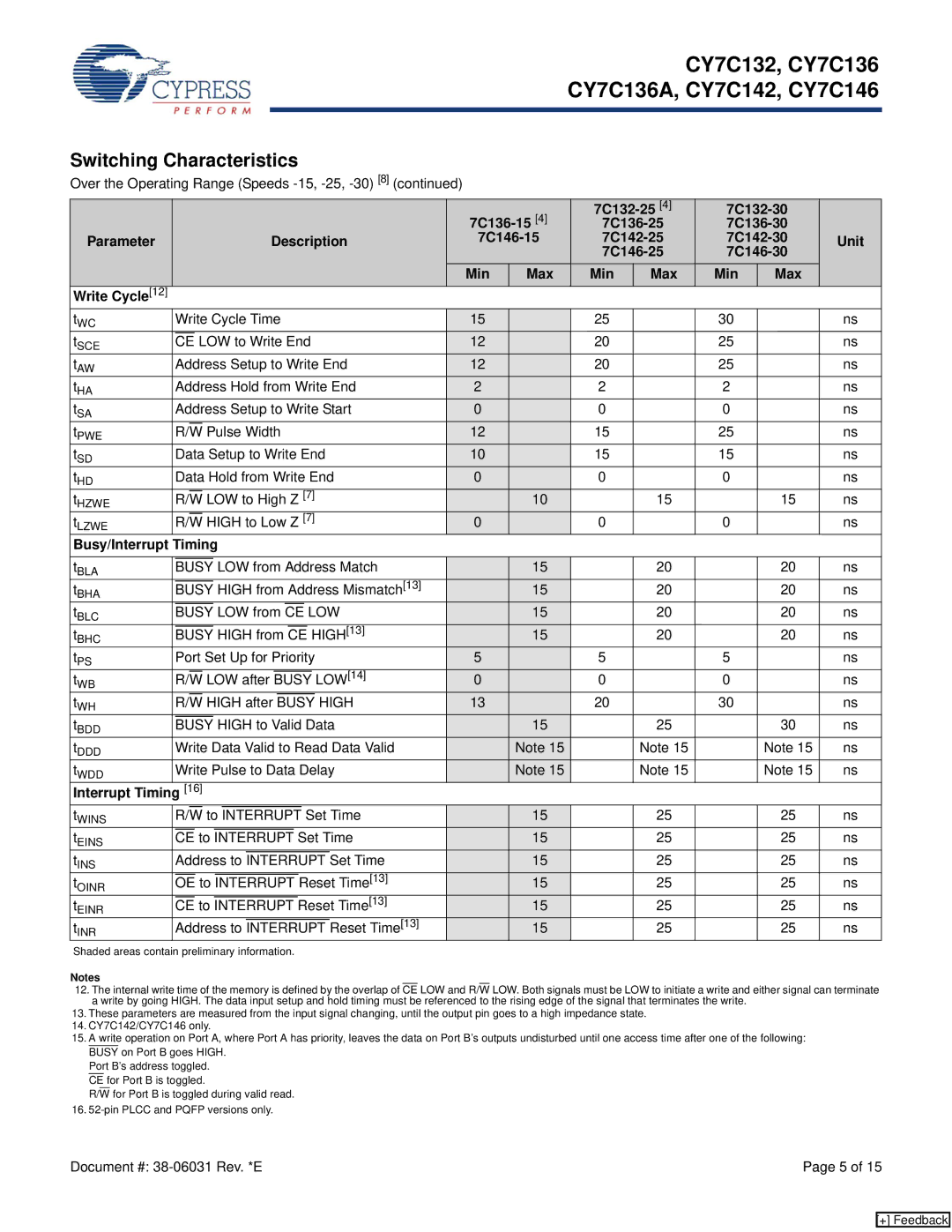
Switching Characteristics
Over the Operating Range (Speeds
|
|
|
|
|
|
|
|
|
|
|
|
|
|
|
|
|
|
|
|
|
|
|
|
|
|
| ||||||
|
|
|
|
|
|
|
|
|
|
|
|
|
|
|
|
|
|
|
|
|
|
|
|
|
|
| ||||||
Parameter |
|
|
|
|
|
|
|
|
|
|
|
| Description | Unit | ||||||||||||||||||
|
|
|
|
|
|
|
|
|
|
|
|
|
|
|
|
|
|
|
|
|
|
|
|
|
|
|
|
| ||||
|
|
|
|
|
|
|
|
|
|
|
|
|
|
|
|
|
|
|
|
|
|
|
|
|
| Min | Max | Min | Max | Min | Max |
|
Write Cycle[12] |
|
|
|
|
|
|
|
|
|
|
|
|
|
|
|
|
|
|
|
|
|
|
|
|
|
|
|
|
|
|
|
|
tWC |
| Write Cycle Time | 15 |
| 25 |
| 30 |
| ns | |||||||||||||||||||||||
tSCE |
| CE |
| LOW to Write End | 12 |
| 20 |
| 25 |
| ns | |||||||||||||||||||||
tAW |
| Address Setup to Write End | 12 |
| 20 |
| 25 |
| ns | |||||||||||||||||||||||
tHA |
| Address Hold from Write End | 2 |
| 2 |
| 2 |
| ns | |||||||||||||||||||||||
tSA |
| Address Setup to Write Start | 0 |
| 0 |
| 0 |
| ns | |||||||||||||||||||||||
tPWE |
|
|
|
|
| Pulse Width | 12 |
| 15 |
| 25 |
| ns | |||||||||||||||||||
R/W |
|
|
| |||||||||||||||||||||||||||||
tSD |
| Data Setup to Write End | 10 |
| 15 |
| 15 |
| ns | |||||||||||||||||||||||
tHD |
| Data Hold from Write End | 0 |
| 0 |
| 0 |
| ns | |||||||||||||||||||||||
tHZWE |
|
|
|
| LOW to High Z [7] |
| 10 |
| 15 |
| 15 | ns | ||||||||||||||||||||
R/W |
|
|
| |||||||||||||||||||||||||||||
tLZWE |
|
|
|
| HIGH to Low Z [7] | 0 |
| 0 |
| 0 |
| ns | ||||||||||||||||||||
R/W |
|
|
| |||||||||||||||||||||||||||||
Busy/Interrupt Timing |
|
|
|
|
|
|
| |||||||||||||||||||||||||
|
|
|
|
|
|
|
|
|
|
|
|
|
|
|
|
|
|
|
|
|
|
|
|
| ||||||||
tBLA |
| BUSY |
|
| LOW from Address Match |
| 15 |
| 20 |
| 20 | ns | ||||||||||||||||||||
tBHA |
| BUSY |
|
| HIGH from Address Mismatch[13] |
| 15 |
| 20 |
| 20 | ns | ||||||||||||||||||||
tBLC |
| BUSY |
|
| LOW from | CE |
| LOW |
| 15 |
| 20 |
| 20 | ns | |||||||||||||||||
tBHC |
| BUSY |
|
| HIGH from | CE | HIGH[13] |
| 15 |
| 20 |
| 20 | ns | ||||||||||||||||||
tPS |
| Port Set Up for Priority | 5 |
| 5 |
| 5 |
| ns | |||||||||||||||||||||||
tWB |
|
|
|
| LOW after |
|
|
|
|
|
| LOW[14] | 0 |
| 0 |
| 0 |
| ns | |||||||||||||
R/W | BUSY |
|
|
| ||||||||||||||||||||||||||||
tWH |
|
|
|
| HIGH after |
|
|
|
| HIGH | 13 |
| 20 |
| 30 |
| ns | |||||||||||||||
R/W | BUSY |
|
|
| ||||||||||||||||||||||||||||
tBDD |
| BUSY |
|
| HIGH to Valid Data |
| 15 |
| 25 |
| 30 | ns | ||||||||||||||||||||
tDDD |
| Write Data Valid to Read Data Valid |
| Note 15 |
| Note 15 |
| Note 15 | ns | |||||||||||||||||||||||
tWDD |
| Write Pulse to Data Delay |
| Note 15 |
| Note 15 |
| Note 15 | ns | |||||||||||||||||||||||
Interrupt Timing | [16] |
|
|
|
|
|
|
| ||||||||||||||||||||||||
|
|
|
|
|
|
|
|
|
|
|
|
|
|
|
|
| ||||||||||||||||
tWINS |
|
|
|
| to |
|
|
|
| Set Time |
| 15 |
| 25 |
| 25 | ns | |||||||||||||||
R/W | INTERRUPT |
|
|
| ||||||||||||||||||||||||||||
tEINS |
| CE |
| to | INTERRUPT |
| Set Time |
| 15 |
| 25 |
| 25 | ns | ||||||||||||||||||
tINS |
| Address to | INTERRUPT | Set Time |
| 15 |
| 25 |
| 25 | ns | |||||||||||||||||||||
tOINR |
| OE | to | INTERRUPT | Reset Time[13] |
| 15 |
| 25 |
| 25 | ns | ||||||||||||||||||||
tEINR |
| CE | to | INTERRUPT | Reset Time[13] |
| 15 |
| 25 |
| 25 | ns | ||||||||||||||||||||
tINR |
| Address to | INTERRUPT | Reset Time[13] |
| 15 |
| 25 |
| 25 | ns | |||||||||||||||||||||
Shaded areas contain preliminary information.
Notes
12.The internal write time of the memory is defined by the overlap of CE LOW and R/W LOW. Both signals must be LOW to initiate a write and either signal can terminate a write by going HIGH. The data input setup and hold timing must be referenced to the rising edge of the signal that terminates the write.
13.These parameters are measured from the input signal changing, until the output pin goes to a high impedance state.
14.CY7C142/CY7C146 only.
15.A write operation on Port A, where Port A has priority, leaves the data on Port B’s outputs undisturbed until one access time after one of the following: BUSY on Port B goes HIGH.
Port B’s address toggled. CE for Port B is toggled.
R/W for Port B is toggled during valid read.
16.
Document #: | Page 5 of 15 |
[+] Feedback