CY7C132, CY7C136
CY7C136A, CY7C142, CY7C146
Switching Waveforms (continued)
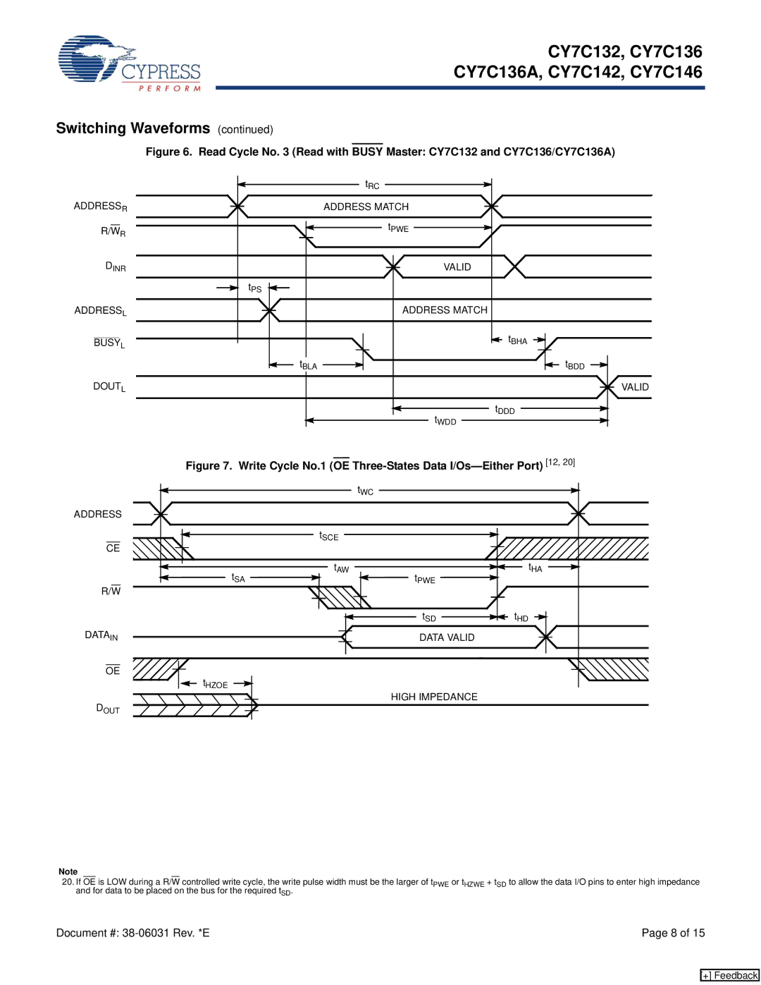
Figure 6. Read Cycle No. 3 (Read with BUSY Master: CY7C132 and CY7C136/CY7C136A)
| tRC |
ADDRESSR | ADDRESS MATCH |
R/WR | tPWE |
DINR | VALID |
tPS |
|
ADDRESSL | ADDRESS MATCH |
BUSYL | tBHA |
tBLA | tBDD |
DOUTL | VALID |
| tDDD |
| tWDD |
Figure 7. Write Cycle No.1 (OE Three-States Data I/Os—Either Port) [12, 20]
| tWC |
|
ADDRESS |
|
|
tSCE |
|
|
CE |
|
|
tAW | tPWE | tHA |
tSA |
| |
R/W |
|
|
| tSD | tHD |
DATAIN | DATA VALID |
|
OE |
|
|
tHZOE | HIGH IMPEDANCE |
|
DOUT |
| |
|
|
Note
20.If OE is LOW during a R/W controlled write cycle, the write pulse width must be the larger of tPWE or tHZWE + tSD to allow the data I/O pins to enter high impedance and for data to be placed on the bus for the required tSD.
Document #: | Page 8 of 15 |
[+] Feedback