CY7C132, CY7C136
CY7C136A, CY7C142, CY7C146
Switching Waveforms (continued)
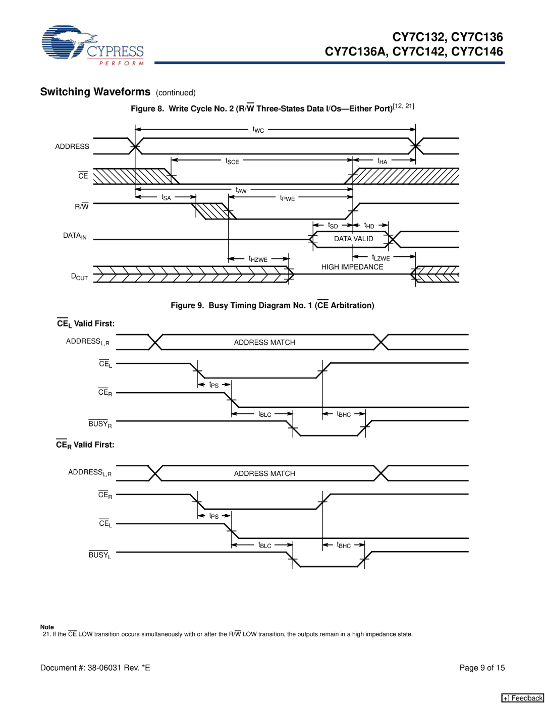
Figure 8. Write Cycle No. 2 (R/W Three-States Data I/Os—Either Port)[12, 21]
| tWC |
|
ADDRESS |
|
|
tSCE |
| tHA |
CE |
|
|
tAW | tPWE |
|
tSA |
| |
R/W |
|
|
| tSD | tHD |
DATAIN | DATA VALID | |
t | HZWE | tLZWE |
|
| |
HIGH IMPEDANCE
DOUT
Figure 9. Busy Timing Diagram No. 1 (CE Arbitration)
CEL Valid First:
ADDRESSL,R
CEL
CER
BUSYR
CER Valid First:
ADDRESSL,R
CER
CEL
BUSYL
ADDRESS MATCH |
|
tPS |
|
tBLC | tBHC |
ADDRESS MATCH
tPS
| tBLC |
|
|
|
|
|
|
| tBHC |
|
|
|
|
|
|
|
|
|
|
| |||||||
|
|
|
|
|
|
|
|
|
|
|
|
|
|
|
|
|
|
|
|
|
|
|
|
|
|
|
|
|
|
|
|
|
|
|
|
|
|
|
|
|
|
|
|
|
|
|
|
|
|
|
|
|
|
|
|
Note
21. If the CE LOW transition occurs simultaneously with or after the R/W LOW transition, the outputs remain in a high impedance state.
Document #: | Page 9 of 15 |
[+] Feedback