CY7C132, CY7C136 CY7C136A, CY7C142, CY7C146
2K x 8 Dual-Port Static RAM
Features
■True
■2K x 8 organization
■0.65 micron CMOS for optimum speed and power
■High speed access: 15 ns
■Low operating power: ICC = 110 mA (maximum)
■Fully asynchronous operation
■Automatic power down
■Master CY7C132/CY7C136/CY7C136A[1] easily expands data bus width to 16 or more bits using slave CY7C142/CY7C146
■BUSY output flag on CY7C132/CY7C136/CY7C136A; BUSY input on CY7C142/CY7C146
■INT flag for port to port communication
■CY7C136, CY7C136A, and CY7C146 available in
■
Functional Description
The CY7C132, CY7C136, CY7C136A, CY7C142, and CY7C146 are high speed CMOS 2K x 8
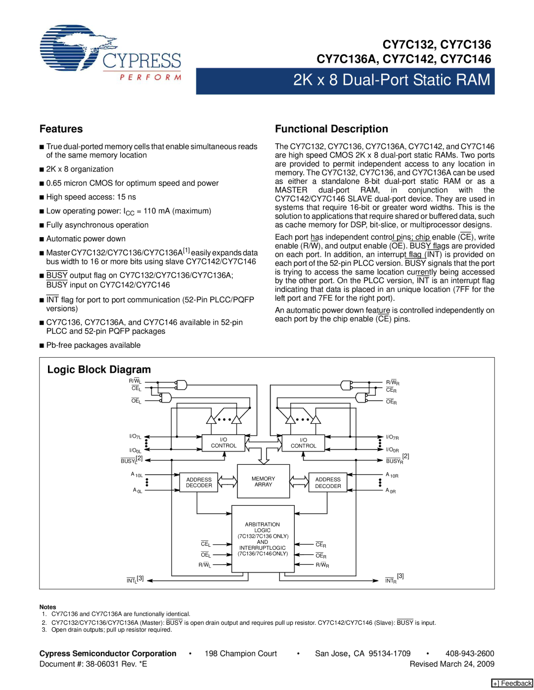
Each port has independent control pins; chip enable (CE), write enable (R/W), and output enable (OE). BUSY flags are provided on each port. In addition, an interrupt flag (INT) is provided on each port of the
An automatic power down feature is controlled independently on each port by the chip enable (CE) pins.
Logic Block Diagram |
|
|
|
|
R/WL |
|
|
| R/WR |
CEL |
|
|
| CER |
OEL |
|
|
| OER |
I/O7L | I/O |
| I/O | I/O7R |
|
|
| ||
I/O0L | CONTROL |
| CONTROL | I/O0R |
|
|
| ||
BUSYL[2] |
|
|
| BUSYR[2] |
A 10L | ADDRESS | MEMORY | ADDRESS | A 10R |
A 0L | DECODER | ARRAY | DECODER | A 0R |
|
|
| ||
|
| ARBITRATION |
|
|
|
| LOGIC |
|
|
|
| (7C132/7C136 ONLY) |
|
|
| CEL | AND | CER |
|
| INTERRUPTLOGIC |
| ||
| OEL | (7C136/7C146 ONLY) | OER |
|
| R/WL |
| R/WR |
|
INTL[3] |
|
|
| INTR[3] |
Notes
1.CY7C136 and CY7C136A are functionally identical.
2.CY7C132/CY7C136/CY7C136A (Master): BUSY is open drain output and requires pull up resistor. CY7C142/CY7C146 (Slave): BUSY is input.
3.Open drain outputs; pull up resistor required.
Cypress Semiconductor Corporation • 198 Champion Court | • | San Jose, CA | • | |
Document #: |
| Revised March 24, 2009 | ||
[+] Feedback