CY7C1324H specifications
The Cypress CY7C1324H is a high-performance SRAM (Static Random Access Memory) device that plays a crucial role in various applications requiring fast and efficient data access. This device is part of the CY7C family of SRAM products and stands out for its advanced features, robust performance metrics, and versatility in operation.One of the most notable features of the CY7C1324H is its 32 megabit (4M x 8) memory capacity, which allows for significant data storage and retrieval capabilities. This memory is organized as a 4M word by 8 bits, making it suitable for a wide range of applications, from automotive to telecommunications and industrial control systems.
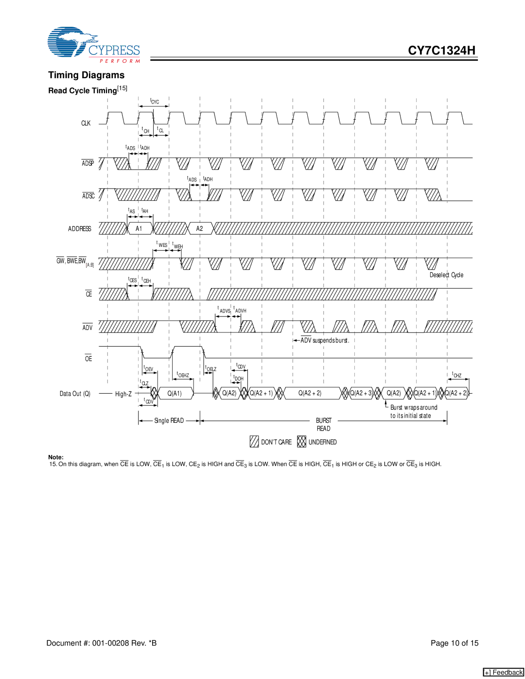
The CY7C1324H operates at a speed of 20 nanoseconds, making it an ideal choice for systems that require rapid read and write cycles. The device supports both asynchronous read and write operations, allowing for flexible interfacing with various microcontrollers and digital signal processors. This speed enhances overall system performance, especially when handling time-critical data.
In terms of technologies, the CY7C1324H employs high-speed CMOS (Complementary Metal-Oxide-Semiconductor) technology, which contributes to its low power consumption and high reliability. The device operates at a voltage range of 2.7V to 3.6V, making it suitable for battery-powered applications where energy efficiency is paramount. The integration of advanced CMOS technology also facilitates a higher degree of integration, enabling more compact designs in electronic circuits.
The device features a simple and straightforward interface, with a single enable (E) control pin that allows for easy access to memory contents. Additionally, the CY7C1324H supports both byte-wide and word-wide data accesses, making it highly adaptable for various application requirements.
Another important characteristic of the CY7C1324H is its low pin count, consisting of only 32 pins, which aids in minimizing board space and simplifying design layouts. The packaging comes in a 44-lead Thin Quad Flat Pack (TQFP), further optimizing space usage in compact electronic designs.
In summary, the Cypress CY7C1324H is a versatile, high-speed SRAM solution that offers a combination of large memory capacity, rapid access times, and low power operation. Its robust features make it an excellent choice for a broad spectrum of electronic applications, paving the way for enhanced performance and efficiency in modern electronic systems.

