CY7C1352G
Document History Page
Document Title: CY7C1352G
Document Number:
REV. | ECN NO. | Issue | Orig. of | Description of Change |
Date | Change | |||
|
|
|
|
|
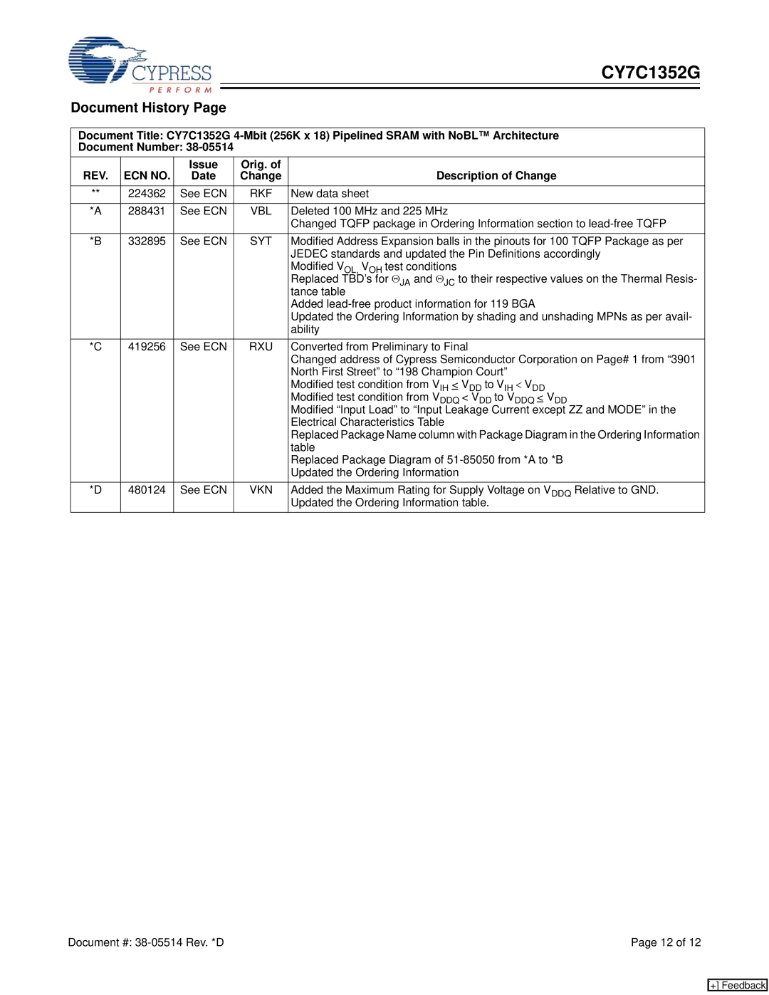
** | 224362 | See ECN | RKF | New data sheet |
|
|
|
|
|
*A | 288431 | See ECN | VBL | Deleted 100 MHz and 225 MHz |
|
|
|
| Changed TQFP package in Ordering Information section to |
*B | 332895 | See ECN | SYT | Modified Address Expansion balls in the pinouts for 100 TQFP Package as per |
|
|
|
| JEDEC standards and updated the Pin Definitions accordingly |
|
|
|
| Modified VOL, VOH test conditions |
|
|
|
| Replaced TBD’s for ΘJA and ΘJC to their respective values on the Thermal Resis- |
|
|
|
| tance table |
|
|
|
| Added |
|
|
|
| Updated the Ordering Information by shading and unshading MPNs as per avail- |
|
|
|
| ability |
*C | 419256 | See ECN | RXU | Converted from Preliminary to Final |
|
|
|
| Changed address of Cypress Semiconductor Corporation on Page# 1 from “3901 |
|
|
|
| North First Street” to “198 Champion Court” |
|
|
|
| Modified test condition from VIH < VDD to VIH < VDD |
|
|
|
| Modified test condition from VDDQ < VDD to VDDQ < VDD |
|
|
|
| Modified “Input Load” to “Input Leakage Current except ZZ and MODE” in the |
|
|
|
| Electrical Characteristics Table |
|
|
|
| Replaced Package Name column with Package Diagram in the Ordering Information |
|
|
|
| table |
|
|
|
| Replaced Package Diagram of |
|
|
|
| Updated the Ordering Information |
*D | 480124 | See ECN | VKN | Added the Maximum Rating for Supply Voltage on VDDQ Relative to GND. |
|
|
|
| Updated the Ordering Information table. |
Document #: | Page 12 of 12 |
[+] Feedback
