Cypress CY7C1413JV18, CY7C1426JV18 Is Referenced With Respect to, TDO for Jtag, TCK Pin for Jtag

Models: CY7C1413JV18 CY7C1426JV18 CY7C1411JV18 CY7C1415JV18

1 28
Download 28 pages 53.11 Kb
Page 7
Image 7


CY7C1411JV18, CY7C1426JV18


CY7C1413JV18, CY7C1415JV18


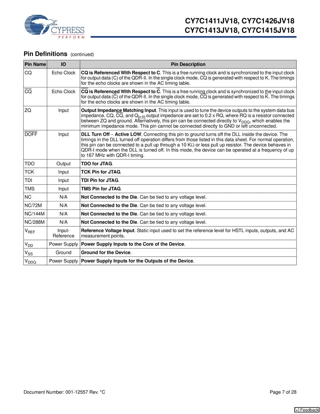
Pin Definitions (continued)


Pin Name

IO


Pin Description


CQ

Echo Clock


CQ is Referenced With Respect to C. This is a free running clock and is synchronized to the input clock


for output data (C) of the QDR-II. In the single clock mode, CQ is generated with respect to K. The timings


for the echo clocks are shown in the AC timing table.


Echo Clock


is Referenced With Respect to


. This is a free running clock and is synchronized to the input clock


CQ


CQ

C


for output data (C) of the QDR-II. In the single clock mode, CQ is generated with respect to K. The timings


for the echo clocks are shown in the AC timing table.


ZQ

Input


Output Impedance Matching Input. This input is used to tune the device outputs to the system data bus


impedance. CQ, CQ, and Q[x:0] output impedance are set to 0.2 x RQ, where RQ is a resistor connected


between ZQ and ground. Alternatively, this pin can be connected directly to VDDQ, which enables the


minimum impedance mode. This pin cannot be connected directly to GND or left unconnected.


Input


DLL Turn Off Active LOW. Connecting this pin to ground turns off the DLL inside the device. The


DOFF


timings in the DLL turned off operation differs from those listed in this data sheet. For normal operation,


this pin can be connected to a pull up through a 10 KΩ or less pull up resistor. The device behaves in


QDR-I mode when the DLL is turned off. In this mode, the device can be operated at a frequency of up


to 167 MHz with QDR-I timing.


TDO

Output


TDO for JTAG.


TCK

Input


TCK Pin for JTAG.


TDI

Input


TDI Pin for JTAG.


TMS

Input


TMS Pin for JTAG.


NC

N/A


Not Connected to the Die. Can be tied to any voltage level.


NC/72M

N/A


Not Connected to the Die. Can be tied to any voltage level.


NC/144M

N/A


Not Connected to the Die. Can be tied to any voltage level.


NC/288M

N/A


Not Connected to the Die. Can be tied to any voltage level.


VREF

Input-


Reference Voltage Input. Static input used to set the reference level for HSTL inputs, outputs, and AC


Reference


measurement points.


VDD

Power Supply


Power Supply Inputs to the Core of the Device.


VSS

Ground


Ground for the Device.


VDDQ

Power Supply


Power Supply Inputs for the Outputs of the Device.

Document Number: 001-12557 Rev. *C

Page 7 of 28

[+] Feedback

Page 7
Image 7
Cypress CY7C1413JV18 Is Referenced With Respect to, TDO for Jtag, TCK Pin for Jtag, TDI Pin for Jtag, TMS Pin for Jtag

CY7C1413JV18, CY7C1426JV18, CY7C1411JV18, CY7C1415JV18 specifications

Cypress Semiconductor, known for its innovative memory solutions, offers a range of high-performance SRAM products suitable for a variety of applications. Among these are the CY7C1415JV18, CY7C1411JV18, CY7C1426JV18, and CY7C1413JV18, which feature advanced technologies and robust performance characteristics.

The CY7C1415JV18 is a 4-Mbit high-speed asynchronous SRAM. Designed for applications requiring fast data access, it boasts a maximum access time of just 10 ns. This product operates at a supply voltage of 1.8V, making it ideal for low-power systems. It supports a simple interface, allowing for easy integration into various digital systems. Enhanced data integrity is assured through support for write cycles and concurrent read operations, making it suitable for high-demand environments.

The CY7C1411JV18 is a 2-Mbit synchronous SRAM that offers high speed and low latency. Its access time is optimized for high-performance applications, reaching speeds of up to 10 ns as well. The device is designed with a flexible interface that accommodates both burst and non-burst operations, increasing data throughput for memory-intensive tasks. Like its counterparts, it operates on a low voltage, ensuring minimal power consumption.

Next, the CY7C1426JV18 also belongs to Cypress's high-performance SRAM family, providing 2-Mbit storage capacity with excellent read and write performance characteristics. This SRAM features an advanced design that supports pipelined operations, allowing multiple memory accesses to occur simultaneously. This feature effectively maximizes data transmission rates, making it particularly appealing for applications needing rapid data processing.

Finally, the CY7C1413JV18 offers 1-Mbit of SRAM capacity optimized for speed and efficiency. With an access time of 9 ns, it is among the fastest products in its category. The device features advanced functionalities enabling compatibility with various hardware configurations, thus facilitating its use in a wide array of embedded systems.

All these SRAM devices feature low power consumption, making them suitable for battery-operated devices and energy-efficient applications. Their ability to operate at lower voltages while maintaining high performance is a key characteristic that aligns with modern design requirements. The combination of speed, low power, and flexibility makes the CY7C1415JV18, CY7C1411JV18, CY7C1426JV18, and CY7C1413JV18 highly sought after in industries ranging from telecommunications to consumer electronics, solidifying Cypress's reputation as a leader in memory solutions.