CY7C1460AV25

CY7C1462AV25

CY7C1464AV25

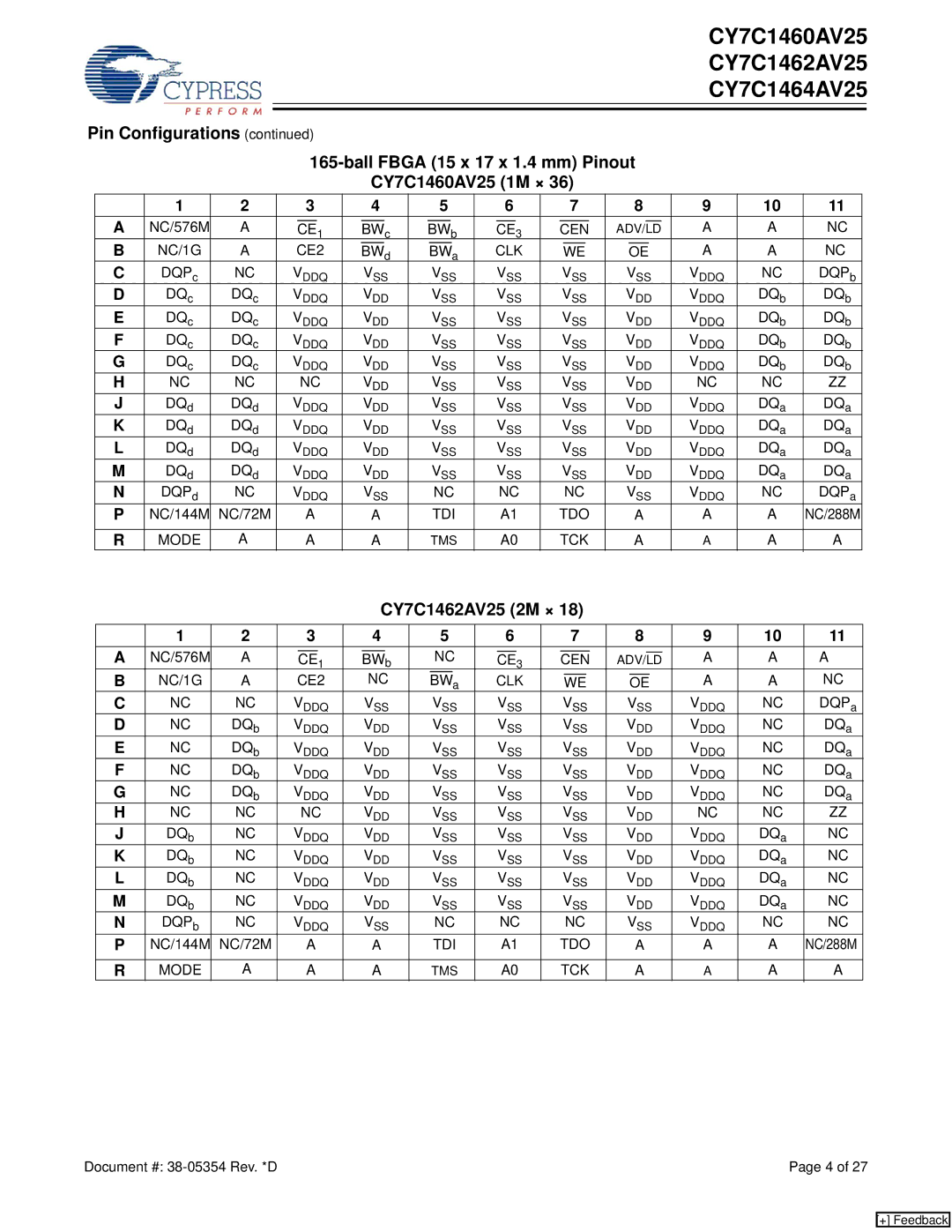
Pin Configurations (continued)

165-ball FBGA (15 x 17 x 1.4 mm) Pinout

CY7C1460AV25 (1M × 36)


1

2

3


4


5


6


7


8


9

10

11

A

NC/576M

A


1


c


b


3


A

A

NC


CE

BW

BW

CE

CEN

ADV/LD


B

NC/1G

A

CE2


d


a

CLK


A

A

NC


BW


BW


WE


OE


C

DQPc

NC

VDDQ


VSS


VSS


VSS


VSS

VSS

VDDQ

NC

DQPb

D

DQc

DQc

VDDQ


VDD


VSS


VSS


VSS

VDD

VDDQ

DQb

DQb

E

DQc

DQc

VDDQ


VDD


VSS


VSS


VSS

VDD

VDDQ

DQb

DQb

F

DQc

DQc

VDDQ


VDD


VSS


VSS


VSS

VDD

VDDQ

DQb

DQb

G

DQc

DQc

VDDQ


VDD


VSS


VSS


VSS

VDD

VDDQ

DQb

DQb

H

NC

NC


NC


VDD


VSS


VSS


VSS

VDD

NC

NC

ZZ

J

DQd

DQd

VDDQ


VDD


VSS


VSS


VSS

VDD

VDDQ

DQa

DQa

K

DQd

DQd

VDDQ


VDD


VSS


VSS


VSS

VDD

VDDQ

DQa

DQa

L

DQd

DQd

VDDQ


VDD


VSS


VSS


VSS

VDD

VDDQ

DQa

DQa

M

DQd

DQd

VDDQ


VDD


VSS


VSS


VSS

VDD

VDDQ

DQa

DQa

N

DQPd

NC

VDDQ


VSS


NC


NC


NC

VSS

VDDQ

NC

DQPa

P

NC/144M

NC/72M


A


A


TDI


A1

TDO


A

A

A

NC/288M


R

MODE

A


A


A


TMS


A0


TCK


A

A

A

A

CY7C1462AV25 (2M × 18)


1

2

3


4


5


6


7


8


9

10

11

A

NC/576M

A


NC


A

A

A


CE

1


BW

b


CE

3


CEN


ADV/LD


B

NC/1G

A

CE2


NC


CLK


A

A

NC


BW


a


WE

OE

C

NC

NC

VDDQ


VSS


VSS


VSS


VSS

VSS

VDDQ

NC

DQPa

D

NC

DQb

VDDQ


VDD


VSS


VSS


VSS

VDD

VDDQ

NC

DQa

E

NC

DQb

VDDQ


VDD


VSS


VSS


VSS

VDD

VDDQ

NC

DQa

F

NC

DQb

VDDQ


VDD


VSS


VSS


VSS

VDD

VDDQ

NC

DQa

G

NC

DQb

VDDQ


VDD


VSS


VSS


VSS

VDD

VDDQ

NC

DQa

H

NC

NC


NC


VDD


VSS


VSS


VSS

VDD

NC

NC

ZZ

J

DQb

NC

VDDQ


VDD


VSS


VSS


VSS

VDD

VDDQ

DQa

NC

K

DQb

NC

VDDQ


VDD


VSS


VSS


VSS

VDD

VDDQ

DQa

NC

L

DQb

NC

VDDQ


VDD


VSS


VSS


VSS

VDD

VDDQ

DQa

NC

M

DQb

NC

VDDQ


VDD


VSS


VSS


VSS

VDD

VDDQ

DQa

NC

N

DQPb

NC

VDDQ


VSS


NC


NC


NC

VSS

VDDQ

NC

NC

P

NC/144M

NC/72M


A


A


TDI


A1

TDO


A

A

A

NC/288M


R

MODE

A


A


A


TMS


A0


TCK


A

A

A

A

Document #: 38-05354 Rev. *D

Page 4 of 27

[+] Feedback

Page 4
Image 4
Cypress CY7C1464AV25, CY7C1460AV25 manual CY7C1462AV25 2M ×

CY7C1462AV25, CY7C1460AV25, CY7C1464AV25 specifications

The Cypress CY7C1464AV25, CY7C1460AV25, and CY7C1462AV25 are a family of high-performance synchronous SRAM devices that have been designed for applications requiring fast memory access and low latency. These memory chips are particularly appealing for systems in telecommunications, networking, and embedded applications due to their versatility and robust performance specifications.

One of the standout features of the CY7C1464AV25 series is their large capacities. The CY7C1464AV25 offers a capacity of 4 Megabits (512 K x 8), making it well-suited for applications that demand ample memory while maintaining high-speed operations. In contrast, the CY7C1460AV25 and CY7C1462AV25 provide slightly smaller capacities of 1 Megabit (128 K x 8) and 2 Megabits (256 K x 8) respectively, catering to varying system memory requirements.

All three devices utilize Cypress's advanced synchronous SRAM technology. This enables the chips to support burst read and write modes, allowing for rapid data transfer rates. The CY7C1464AV25 delivers a data access time of as low as 5.5 ns, making it highly efficient for data-intensive applications. Additionally, the standard operating voltage of 2.5V aids in reducing power consumption and improving overall system energy efficiency.

The chips are also characterized by a simple interface and compatibility with common bus protocols, which facilitates easy integration into existing systems. They feature a dual-port architecture, allowing multiple data transfers to occur simultaneously, significantly improving throughput.

With a commercial temperature range, all three devices offer reliability and are suited for a wide range of operating environments. The package options include a compact 44-pin TSOP, allowing for space-saving designs in modern electronics.

In summary, the Cypress CY7C1464AV25, CY7C1460AV25, and CY7C1462AV25 provide a powerful blend of capacity, speed, and efficiency, making them ideal choices for demanding applications in various sectors. Their advanced technologies and versatility make them excellent candidates for enhancing system performance while maintaining low power consumption and ensuring reliable operation in various conditions.