CY7C1471V33
CY7C1473V33
CY7C1475V33
signal while in transition (metastable state). This does not harm the device, but there is no guarantee as to the value that is captured. Repeatable results may not be possible.
To guarantee that the boundary scan register captures the correct value of a signal, the SRAM signal must be stabilized long enough to meet the TAP controller’s capture setup plus hold time (tCS plus tCH).
The SRAM clock input might not be captured correctly if there is no way in a design to stop (or slow) the clock during a SAMPLE/PRELOAD instruction. If this is an issue, it is still possible to capture all other signals and simply ignore the value of the CLK captured in the boundary scan register.
After the data is captured, it is possible to shift out the data by putting the TAP into the
Note that since the PRELOAD part of the command is not implemented, putting the TAP to the
BYPASS
When the BYPASS instruction is loaded in the instruction register and the TAP is placed in a
Reserved
These instructions are not implemented but are reserved for future use. Do not use these instructions.
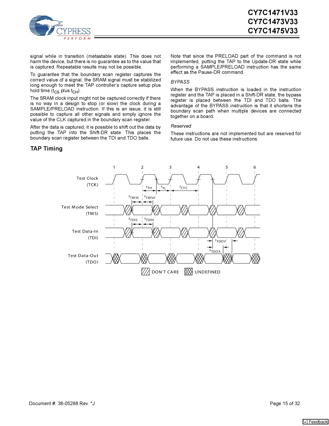
TAP Timing
1 | 2 |
| 3 |
Test Clock |
|
|
|
(TCK ) | tTH | tTL | tCY C |
| |||
tTM SS | tTM SH |
|
|
Test M ode Select (TM S)
tTDIS tTDIH
Test
Test
![]() DON’T CA RE
DON’T CA RE
4 | 5 | 6 |
|
|
|
tTDO V
tTDOX
UNDEFINED
Document #: | Page 15 of 32 |
[+] Feedback