CY7C1471V33
CY7C1473V33
CY7C1475V33
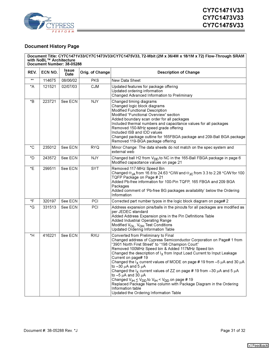
Document History Page
Document Title: CY7C1471V33/CY7C1473V33/CY7C1475V33,
Document Number:
REV. | ECN NO. | Issue | Orig. of Change | Description of Change | |
Date | |||||
|
|
|
| ||
|
|
|
|
| |
** | 114675 | 08/06/02 | PKS | New Data Sheet | |
|
|
|
|
| |
*A | 121521 | 02/07/03 | CJM | Updated features for package offering | |
|
|
|
| Updated ordering information | |
|
|
|
| Changed Advanced Information to Preliminary | |
*B | 223721 | See ECN | NJY | Changed timing diagrams | |
|
|
|
| Changed logic block diagrams | |
|
|
|
| Modified Functional Description | |
|
|
|
| Modified “Functional Overview” section | |
|
|
|
| Added boundary scan order for all packages | |
|
|
|
| Included thermal numbers and capacitance values for all packages | |
|
|
|
| Removed | |
|
|
|
| Included ISB and IDD values | |
|
|
|
| Changed package outline for 165FBGA package and | |
|
|
|
| Removed | |
*C | 235012 | See ECN | RYQ | Minor Change: The data sheets do not match on the spec system and | |
|
|
|
| external web | |
*D | 243572 | See ECN | NJY | Changed ball H2 from VDD to NC in the | |
|
|
|
| Modified capacitance values on page 21 | |
*E | 299511 | See ECN | SYT | Removed | |
|
|
|
| Changed ΘJA from 16.8 to 24.63 °C/W and ΘJC from 3.3 to 2.28 °C/W for 100 | |
|
|
|
| TQFP Package on Page # 21 | |
|
|
|
| Added | |
|
|
|
| Packages | |
|
|
|
| Added comment of | |
|
|
|
| Information | |
*F | 320197 | See ECN | PCI | Corrected part number typos in the logic block diagram on page# 2 | |
|
|
|
|
| |
*G | 331513 | See ECN | PCI | Address expansion pins/balls in the pinouts for all packages are modified as | |
|
|
|
| per JEDEC standard | |
|
|
|
| Added Address Expansion pins in the Pin Definitions Table | |
|
|
|
| Added Industrial Operating Range | |
|
|
|
| Modified VOL, VOH Test Conditions | |
|
|
|
| Updated Ordering Information Table | |
*H | 416221 | See ECN | RXU | Converted from Preliminary to Final | |
|
|
|
| Changed address of Cypress Semiconductor Corporation on Page# 1 from | |
|
|
|
| “3901 North First Street” to “198 Champion Court” | |
|
|
|
| Removed 100MHz Speed bin & Added 117MHz Speed bin | |
|
|
|
| Changed the description of IX from Input Load Current to Input Leakage | |
|
|
|
| Current on page# 19 | |
|
|
|
| Changed the IX current values of MODE on page # 19 from | |
|
|
|
| to | |
|
|
|
| Changed the IX current values of ZZ on page # 19 from | |
|
|
|
| to | |
|
|
|
| Changed VIH < VDD to VIH < VDD on page # 19 | |
|
|
|
| Replaced Package Name column with Package Diagram in the Ordering | |
|
|
|
| Information table | |
|
|
|
| Updated the Ordering Information Table |
Document #: | Page 31 of 32 |
[+] Feedback