CY7C1471V33
CY7C1473V33
CY7C1475V33
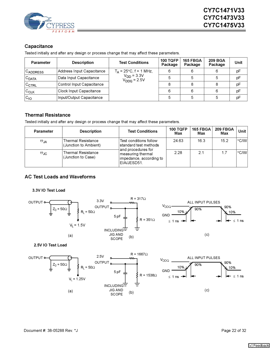
Capacitance
Tested initially and after any design or process change that may affect these parameters.
Parameter | Description | Test Conditions | 100 TQFP | 165 FBGA | 209 BGA | Unit | |
Package | Package | Package | |||||
|
|
|
| ||||
|
|
|
|
|
|
| |
CADDRESS | Address Input Capacitance | TA = 25°C, f = 1 MHz, | 6 | 6 | 6 | pF | |
|
| VDD = 3.3V |
|
|
|
| |
CDATA | Data Input Capacitance | 5 | 5 | 5 | pF | ||
VDDQ = 2.5V | |||||||
CCTRL | Control Input Capacitance | 8 | 8 | 8 | pF | ||
| |||||||
CCLK | Clock Input Capacitance |
| 6 | 6 | 6 | pF | |
CIO | Input/Output Capacitance |
| 5 | 5 | 5 | pF |
Thermal Resistance
Tested initially and after any design or process change that may affect these parameters.
Parameter | Description | Test Conditions | 100 TQFP | 165 FBGA | 209 FBGA | Unit | |
|
|
| Max | Max | Max |
| |
ΘJA | Thermal Resistance | Test conditions follow | 24.63 | 16.3 | 15.2 | °C/W | |
| (Junction to Ambient) | standard test methods |
|
|
|
| |
|
| and procedures for |
|
|
|
| |
ΘJC | Thermal Resistance | 2.28 | 2.1 | 1.7 | °C/W | ||
measuring thermal | |||||||
| (Junction to Case) | impedance, according to |
|
|
|
| |
|
| EIA/JESD51. |
|
|
|
| |
|
|
|
|
|
|
|
AC Test Loads and Waveforms
3.3V IO Test Load
OUTPUT |
|
|
|
|
|
|
|
|
|
|
|
|
| 3.3V |
|
|
| R = 317Ω |
|
|
|
|
| ALL INPUT PULSES | ||||||||||||||||||||
|
|
|
|
|
|
|
|
|
|
|
|
|
|
|
|
|
|
|
|
|
|
|
| VDDQ |
|
|
|
| ||||||||||||||||
|
|
|
|
|
| Z0 | = 50Ω |
|
|
|
| OUTPUT |
|
|
|
|
|
|
|
|
|
|
|
|
|
|
|
|
|
|
|
|
|
| ||||||||||
|
|
|
|
|
|
| RL | = 50Ω |
|
|
|
|
|
|
|
|
|
|
|
|
| 10% |
|
|
|
|
|
| 90% |
|
| |||||||||||||
|
|
|
|
|
|
|
|
|
|
|
|
|
|
|
|
|
|
|
|
|
|
|
|
|
|
|
|
|
|
|
|
|
|
|
| |||||||||
|
|
|
|
|
|
|
|
|
|
|
|
|
|
| 5 pF |
|
|
|
|
|
|
|
|
|
|
|
|
|
| R = 351Ω | GND |
|
|
|
|
|
|
|
|
|
|
| ||
|
|
|
|
|
|
|
|
|
|
|
|
|
|
|
|
|
|
|
|
|
|
|
|
|
|
|
|
|
|
|
|
|
|
|
|
|
| |||||||
|
|
|
|
|
|
|
|
|
|
|
|
|
|
|
|
|
|
|
|
|
|
|
|
|
|
|
|
|
|
| ≤ 1 ns |
|
|
|
|
|
|
|
|
| ||||
|
|
|
|
|
|
|
|
|
| VL = 1.5V |
|
|
|
|
|
|
|
|
|
|
|
|
|
|
|
|
|
|
|
|
|
|
|
|
|
| ||||||||
|
|
|
|
|
|
|
|
|
|
|
|
|
|
|
|
|
|
|
|
|
|
|
|
|
|
|
|
|
|
|
|
|
|
|
|
| ||||||||
|
|
|
|
|
|
|
|
|
|
|
|
|
|
|
|
|
|
|
|
|
|
|
|
|
|
|
|
|
|
|
|
|
|
|
|
|
|
|
|
| ||||
|
|
|
|
|
|
|
|
|
|
|
|
|
| INCLUDING |
|
|
|
|
|
|
|
|
|
|
|
|
|
|
|
|
|
|
|
|
|
|
|
|
| (c) | ||||
|
|
|
|
|
|
|
|
|
|
|
|
|
|
|
|
|
|
|
|
|
|
|
|
|
|
|
|
|
|
|
|
|
|
|
|
|
|
|
| |||||
|
|
|
|
|
|
|
|
|
|
|
|
|
|
|
|
|
|
|
|
|
|
|
|
|
|
|
|
|
|
|
|
|
|
|
|
|
|
|
| |||||
|
|
|
|
|
|
|
|
| (a) | JIG AND |
| (b) |
|
|
|
|
|
|
|
|
|
| ||||||||||||||||||||||
|
|
|
|
|
|
|
|
|
|
|
|
|
| SCOPE |
|
|
|
|
|
|
|
|
|
|
|
|
|
| ||||||||||||||||
|
|
|
|
|
|
|
|
|
|
|
|
|
|
|
|
|
|
|
|
|
|
|
|
|
|
|
|
|
|
|
|
|
|
|
|
|
| |||||||
2.5V IO Test Load |
|
|
|
|
|
|
|
|
|
|
|
|
|
|
|
|
|
|
|
|
|
|
|
|
|
|
|
|
|
|
| |||||||||||||
OUTPUT |
|
|
|
|
|
|
|
|
|
|
|
|
| 2.5V |
|
|
| R = 1667Ω |
|
|
|
|
| ALL INPUT PULSES | ||||||||||||||||||||
|
|
|
|
|
|
|
|
|
|
|
|
|
|
|
|
|
|
|
|
|
|
|
| VDDQ |
|
|
|
| ||||||||||||||||
|
|
|
|
|
| Z0 | = 50Ω |
|
|
|
| OUTPUT |
|
|
|
|
|
|
|
|
|
|
|
|
|
|
|
|
|
|
|
|
|
| ||||||||||
|
|
|
|
|
|
| RL | = 50Ω |
|
|
|
|
|
|
|
|
|
|
|
|
| 10% |
|
|
| 90% |
|
| ||||||||||||||||
|
|
|
|
|
|
|
|
|
|
|
|
|
|
|
|
|
|
|
|
|
|
|
|
|
|
|
|
|
|
|
|
|
|
|
| |||||||||
|
|
|
|
|
|
|
|
|
|
|
|
|
|
| 5 pF |
|
|
|
|
|
|
|
|
|
|
|
|
|
| R = 1538Ω | GND |
|
|
|
|
|
|
|
|
|
| |||
|
|
|
|
|
|
|
|
|
|
|
|
|
|
|
|
|
|
|
|
|
|
|
|
|
|
|
|
|
|
|
|
|
|
|
|
|
| |||||||
|
|
|
|
|
|
|
|
|
|
|
|
|
|
|
|
|
|
|
|
|
|
|
|
|
|
|
|
|
|
| ≤ 1 ns |
|
|
|
|
|
|
|
|
| ||||
|
|
|
|
|
|
|
|
|
| VL = 1.25V |
|
|
|
|
|
|
|
|
|
|
|
|
|
|
|
|
|
|
|
|
| |||||||||||||
|
|
|
|
|
|
|
|
|
|
|
|
|
|
|
|
|
|
|
|
|
|
|
|
|
|
|
|
|
|
|
| |||||||||||||
|
|
|
|
|
|
|
|
|
|
|
|
|
|
|
|
|
|
|
|
|
|
|
|
|
|
|
|
|
|
|
|
|
|
| ||||||||||
|
|
|
|
|
|
|
|
|
|
|
|
|
| INCLUDING |
|
|
|
|
|
|
|
|
|
|
|
|
|
|
|
|
|
|
|
|
|
| (c) | |||||||
|
|
|
|
|
|
|
|
|
|
|
|
|
|
|
|
|
|
|
|
|
|
|
|
|
|
|
|
|
|
|
|
|
|
|
|
|
|
|
| |||||
|
|
|
|
|
|
|
|
|
|
|
|
|
|
|
|
|
|
|
|
|
|
|
|
|
|
|
|
|
|
|
|
|
|
|
|
|
|
|
| |||||
|
|
|
|
|
|
|
|
| (a) | JIG AND |
| (b) |
|
|
|
|
|
|
|
|
|
| ||||||||||||||||||||||
|
|
|
|
|
|
|
|
|
|
|
|
|
| SCOPE |
|
|
|
|
|
|
|
|
|
|
|
|
|
| ||||||||||||||||
|
|
|
|
|
|
|
|
|
|
|
|
|
|
|
|
|
|
|
|
|
|
|
|
|
|
|
|
|
|
|
|
|
|
|
|
|
| |||||||
90%
10%
≤ 1 ns
90%
10%
≤ 1 ns
Document #: | Page 22 of 32 |
[+] Feedback