CY7C1511V18, CY7C1526V18
CY7C1513V18, CY7C1515V18
Document History Page
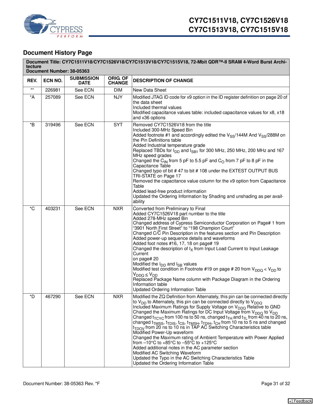
Document Title: CY7C1511V18/CY7C1526V18/CY7C1513V18/CY7C1515V18, | ||||
tecture |
|
|
|
|
Document Number: |
|
| ||
REV. | ECN NO. | SUBMISSION | ORIG. OF | DESCRIPTION OF CHANGE |
DATE | CHANGE | |||
** | 226981 | See ECN | DIM | New Data Sheet |
|
|
|
|
|
*A | 257089 | See ECN | NJY | Modified JTAG ID code for x9 option in the ID register definition on page 20 of |
|
|
|
| the data sheet |
|
|
|
| Included thermal values |
|
|
|
| Modified capacitance values table: included capacitance values for x8, x18 |
|
|
|
| and x36 options |
*B | 319496 | See ECN | SYT | Removed CY7C1526V18 from the title |
|
|
|
| Included |
|
|
|
| Added footnote #1 and accordingly edited the VSS/144M And VSS/288M on |
|
|
|
| the Pin Definitions table |
|
|
|
| Added Industrial temperature grade |
|
|
|
| Replaced TBDs for IDD and ISB1 for 300 MHz, 250 MHz, 200 MHz and 167 |
|
|
|
| MHz speed grades |
|
|
|
| Changed the CIN from 5 pF to 5.5 pF and CO from 7 pF to 8 pF in the |
|
|
|
| Capacitance Table |
|
|
|
| Changed typo of bit # 47 to bit # 108 under the EXTEST OUTPUT BUS |
|
|
|
| |
|
|
|
| Removed the capacitance value column for the x9 option from Capacitance |
|
|
|
| Table |
|
|
|
| Added |
|
|
|
| Updated the Ordering Information by Shading and unshading as per avail- |
|
|
|
| ability |
*C | 403231 | See ECN | NXR | Converted from Preliminary to Final |
|
|
|
| Added CY7C1526V18 part number to the title |
|
|
|
| Added |
|
|
|
| Changed address of Cypress Semiconductor Corporation on Page# 1 from |
|
|
|
| “3901 North First Street” to “198 Champion Court” |
|
|
|
| Changed C/C Pin Description in the features section and Pin Description |
|
|
|
| Added |
|
|
|
| Added foot notes #16, 17, 18 on page# 19 |
|
|
|
| Changed the description of IX from Input Load Current to Input Leakage |
|
|
|
| Current |
|
|
|
| on page# 20 |
|
|
|
| Modified the IDD and ISB values |
|
|
|
| Modified test condition in Footnote #19 on page # 20 from VDDQ < VDD to |
|
|
|
| VDDQ < VDD |
|
|
|
| Replaced Package Name column with Package Diagram in the Ordering |
|
|
|
| Information table |
|
|
|
| Updated Ordering Information Table |
*D | 467290 | See ECN | NXR | Modified the ZQ Definition from Alternately, this pin can be connected directly |
|
|
|
| to VDD to Alternately, this pin can be connected directly to VDDQ |
|
|
|
| Included Maximum Ratings for Supply Voltage on VDDQ Relative to GND |
|
|
|
| Changed the Maximum Ratings for DC Input Voltage from VDDQ to VDD |
|
|
|
| Changed tTCYC from 100 ns to 50 ns, changed tTH and tTL from 40 ns to 20 ns, |
|
|
|
| changed tTMSS, tTDIS, tCS, tTMSH, tTDIH, tCH from 10 ns to 5 ns and changed |
|
|
|
| tTDOV from 20 ns to 10 ns in TAP AC Switching Characteristics table |
|
|
|
| Modified |
|
|
|
| Changed the Maximum rating of Ambient Temperature with Power Applied |
|
|
|
| from |
|
|
|
| Added additional notes in the AC parameter section |
|
|
|
| Modified AC Switching Waveform |
|
|
|
| Updated the Typo in the AC Switching Characteristics Table |
|
|
|
| Updated the Ordering Information Table |
Document Number: |
| Page 31 of 32 | ||
[+] Feedback
