Contents
Main
72-Mbit QDR-II SRAM 4-Word Burst Architecture
CY7C1511V18, CY7C1526V18 CY7C1513V18, CY7C1515V18
Features
Configurations
Functional Description
CY7C1511V18, CY7C1526V18
Document Number: 38-05363 Rev. *F Page 2 of 32
Logic Block Diagram (CY7C1511V18)
Logic Block Diagram (CY7C1526V18)
CY7C1513V18, CY7C1515V18
Document Number: 38-05363 Rev. *F Page 3 of 32
Logic Block Diagram (CY7C1513V18)
Logic Block Diagram (CY7C1515V18)
Pin Configuration
165-Ball FBGA (15 x 17 x 1.4 mm) Pinout
CY7C1511V18, CY7C1526V18 CY7C1513V18, CY7C1515V18
Pin Configuration
165-Ball FBGA (15 x 17 x 1.4 mm) Pinout
CY7C1511V18, CY7C1526V18
Pin Definitions
CY7C1511V18, CY7C1526V18 CY7C1513V18, CY7C1515V18
V V
Pin Definitions
CY7C1511V18, CY7C1526V18 CY7C1513V18, CY7C1515V18
Functional Overview
Read Operations
Write Operations
Byte Write Operations
Concurrent Transactions
Depth Expansion
Programmable Impedance
Echo Clocks
DLL
Application Example
Truth Table
SRAM #4
SRAM #1
BUS MASTER (CPU or ASIC)
CY7C1511V18, CY7C1526V18
Page
CY7C1513V18, CY7C1515V18
IEEE 1149.1 Serial Boundary Scan (JTAG)
Disabling the JTAG Feature
Test Access PortTest Clock
Test Mode Select (TMS)
Page
CY7C1511V18, CY7C1526V18 CY7C1513V18, CY7C1515V18
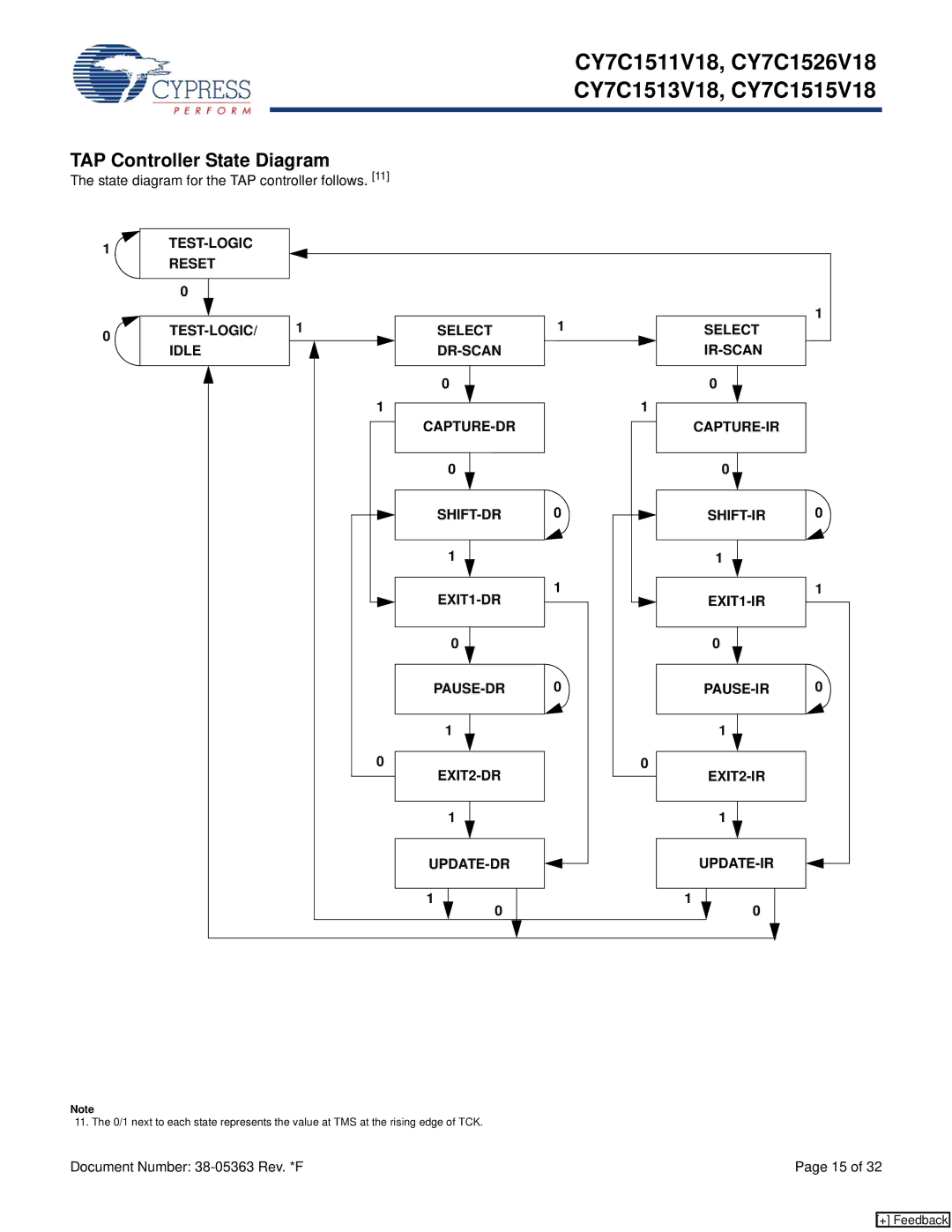
TAP Controller State Diagram
TAP Controller Block Diagram
TAP Electrical Characteristics
TAP AC Switching Characteristics
TAP Timing and Test Conditions
CY7C1511V18, CY7C1526V18 CY7C1513V18, CY7C1515V18
Identification Register Definitions
Scan Register Sizes
Instruction Codes
Boundary Scan Order
Power Up Sequence in QDR-II SRAM
VV
Power Up Sequence
DLL Constraints
/
Maximum Ratings
Operating Range
Electrical Characteristics
DC Electrical Characteristics
AC Electrical Characteristics
Electrical Characteristics
DC Electrical Characteristics
Capacitance
Thermal Resistance
Page
Switching Characteristics
CY7C1511V18, CY7C1526V18
Switching Waveforms
READ READWRITE WRITE
12345
67
Page
Page
Ordering Information
Document Number: 38-05363 Rev. *F Page 30 of 32
Package Diagram
[+] Feedback
Figure 6. 165-ball FBGA (15 x 17 x 1.4 mm), 51-85195
51-85195-*A
Document History Page
Sales, Solutions, and Legal Information
Worldwide Sales and Design Support
Products
PSoC Solutions
Document History Page