CY7C1516JV18, CY7C1527JV18
CY7C1518JV18, CY7C1520JV18
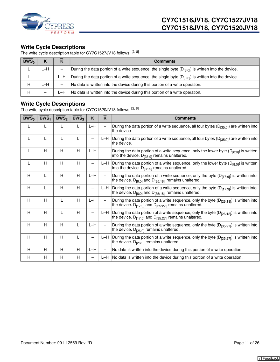
Write Cycle Descriptions
The write cycle description table for CY7C1527JV18 follows. [2, 8]
BWS0 | K | K | Comments |
L | – | During the data portion of a write sequence, the single byte (D[8:0]) is written into the device. | |
L | – | During the data portion of a write sequence, the single byte (D[8:0]) is written into the device. | |
H | – | No data is written into the device during this portion of a write operation. | |
|
|
|
|
H | – | No data is written into the device during this portion of a write operation. | |
|
|
|
|
Write Cycle Descriptions
The write cycle description table for CY7C1520JV18 follows. [2, 8]
| BWS0 |
| BWS1 |
| BWS2 |
| BWS3 | K |
| K | Comments | |||||
| L |
| L |
| L |
| L |
| – | During the data portion of a write sequence, all four bytes (D[35:0]) are written into | ||||||
|
|
|
|
|
|
|
|
|
|
|
|
|
|
|
| the device. |
| L |
| L |
| L |
| L | – | During the data portion of a write sequence, all four bytes (D[35:0]) are written into | |||||||
|
|
|
|
|
|
|
|
|
|
|
|
|
|
|
| the device. |
| L |
| H |
| H |
| H |
| – | During the data portion of a write sequence, only the lower byte (D[8:0]) is written | ||||||
|
|
|
|
|
|
|
|
|
|
|
|
|
|
|
| into the device. D[35:9] remains unaltered. |
| L |
| H |
| H |
| H | – | During the data portion of a write sequence, only the lower byte (D[8:0]) is written | |||||||
|
|
|
|
|
|
|
|
|
|
|
|
|
|
|
| into the device. D[35:9] remains unaltered. |
| H |
| L |
| H |
| H |
| – | During the data portion of a write sequence, only the byte (D[17:9]) is written into | ||||||
|
|
|
|
|
|
|
|
|
|
|
|
|
|
|
| the device. D[8:0] and D[35:18] remains unaltered. |
| H |
| L |
| H |
| H | – | During the data portion of a write sequence, only the byte (D[17:9]) is written into | |||||||
|
|
|
|
|
|
|
|
|
|
|
|
|
|
|
| the device. D[8:0] and D[35:18] remains unaltered. |
| H |
| H |
| L |
| H |
| – | During the data portion of a write sequence, only the byte (D[26:18]) is written into | ||||||
|
|
|
|
|
|
|
|
|
|
|
|
|
|
|
| the device. D[17:0] and D[35:27] remains unaltered. |
| H |
| H |
| L |
| H | – | During the data portion of a write sequence, only the byte (D[26:18]) is written into | |||||||
|
|
|
|
|
|
|
|
|
|
|
|
|
|
|
| the device. D[17:0] and D[35:27] remains unaltered. |
| H |
| H |
| H |
| L |
| – | During the data portion of a write sequence, only the byte (D[35:27]) is written into | ||||||
|
|
|
|
|
|
|
|
|
|
|
|
|
|
|
| the device. D[26:0] remains unaltered. |
| H |
| H |
| H |
| L | – | During the data portion of a write sequence, only the byte (D[35:27]) is written into | |||||||
|
|
|
|
|
|
|
|
|
|
|
|
|
|
|
| the device. D[26:0] remains unaltered. |
| H |
| H |
| H |
| H |
| – | No data is written into the device during this portion of a write operation. | ||||||
|
|
|
|
|
|
|
|
|
|
| ||||||
| H |
| H |
| H |
| H | – | No data is written into the device during this portion of a write operation. | |||||||
|
|
|
|
|
|
|
|
|
|
|
|
|
|
|
|
|
Document Number: | Page 11 of 26 |
[+] Feedback