CY7C1541V18, CY7C1556V18
CY7C1543V18, CY7C1545V18
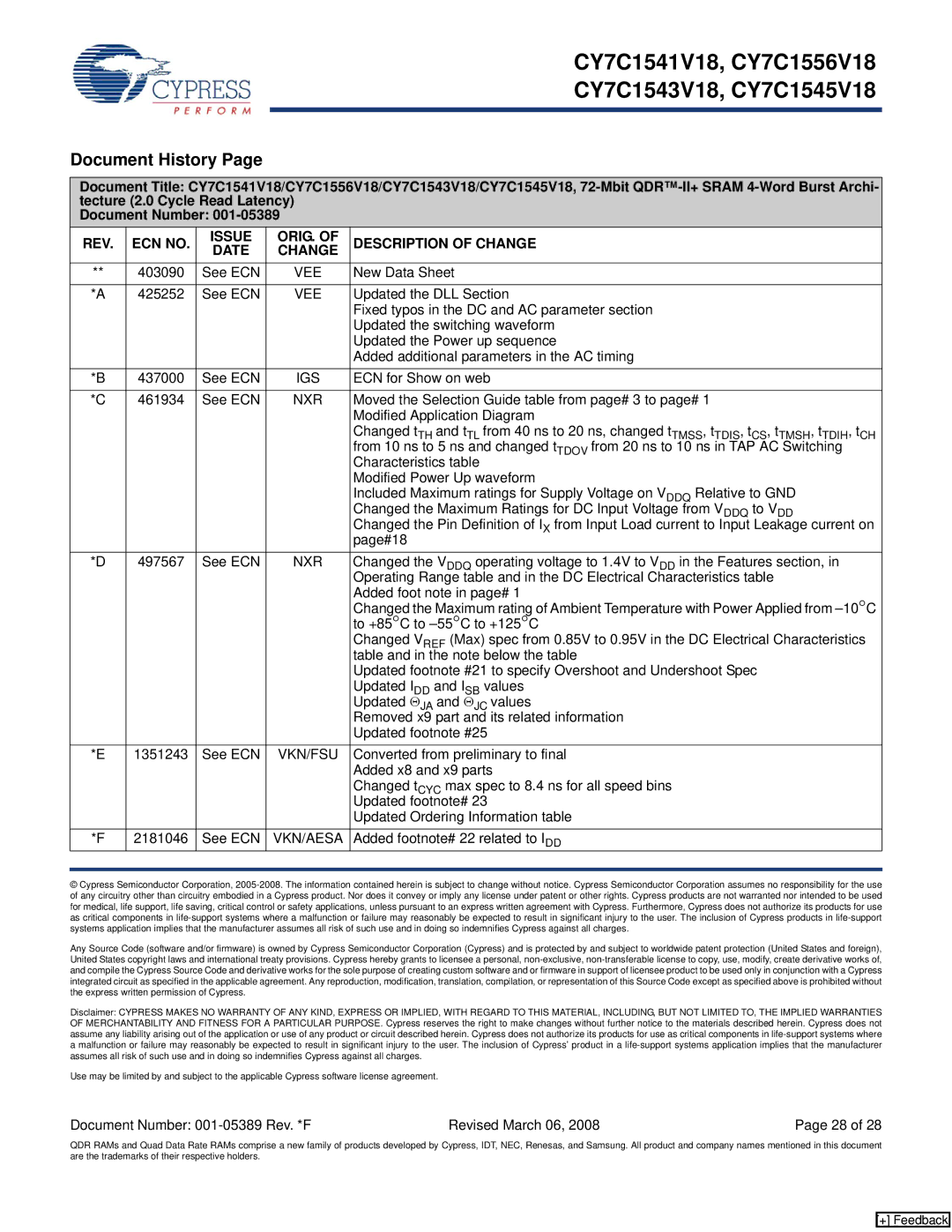
Document History Page
Document Title: CY7C1541V18/CY7C1556V18/CY7C1543V18/CY7C1545V18,
Document Number:
REV. | ECN NO. | ISSUE | ORIG. OF | DESCRIPTION OF CHANGE |
DATE | CHANGE | |||
|
|
|
|
|
** | 403090 | See ECN | VEE | New Data Sheet |
|
|
|
|
|
*A | 425252 | See ECN | VEE | Updated the DLL Section |
|
|
|
| Fixed typos in the DC and AC parameter section |
|
|
|
| Updated the switching waveform |
|
|
|
| Updated the Power up sequence |
|
|
|
| Added additional parameters in the AC timing |
*B | 437000 | See ECN | IGS | ECN for Show on web |
|
|
|
|
|
*C | 461934 | See ECN | NXR | Moved the Selection Guide table from page# 3 to page# 1 |
|
|
|
| Modified Application Diagram |
|
|
|
| Changed tTH and tTL from 40 ns to 20 ns, changed tTMSS, tTDIS, tCS, tTMSH, tTDIH, tCH |
|
|
|
| from 10 ns to 5 ns and changed tTDOV from 20 ns to 10 ns in TAP AC Switching |
|
|
|
| Characteristics table |
|
|
|
| Modified Power Up waveform |
|
|
|
| Included Maximum ratings for Supply Voltage on VDDQ Relative to GND |
|
|
|
| Changed the Maximum Ratings for DC Input Voltage from VDDQ to VDD |
|
|
|
| Changed the Pin Definition of IX from Input Load current to Input Leakage current on |
|
|
|
| page#18 |
*D | 497567 | See ECN | NXR | Changed the VDDQ operating voltage to 1.4V to VDD in the Features section, in |
|
|
|
| Operating Range table and in the DC Electrical Characteristics table |
|
|
|
| Added foot note in page# 1 |
|
|
|
| Changed the Maximum rating of Ambient Temperature with Power Applied from |
|
|
|
| to +85°C to |
|
|
|
| Changed VREF (Max) spec from 0.85V to 0.95V in the DC Electrical Characteristics |
|
|
|
| table and in the note below the table |
|
|
|
| Updated footnote #21 to specify Overshoot and Undershoot Spec |
|
|
|
| Updated IDD and ISB values |
|
|
|
| Updated ΘJA and ΘJC values |
|
|
|
| Removed x9 part and its related information |
|
|
|
| Updated footnote #25 |
*E | 1351243 | See ECN | VKN/FSU | Converted from preliminary to final |
|
|
|
| Added x8 and x9 parts |
|
|
|
| Changed tCYC max spec to 8.4 ns for all speed bins |
|
|
|
| Updated footnote# 23 |
|
|
|
| Updated Ordering Information table |
*F | 2181046 | See ECN | VKN/AESA | Added footnote# 22 related to IDD |
|
|
|
|
|
© Cypress Semiconductor Corporation,
Any Source Code (software and/or firmware) is owned by Cypress Semiconductor Corporation (Cypress) and is protected by and subject to worldwide patent protection (United States and foreign), United States copyright laws and international treaty provisions. Cypress hereby grants to licensee a personal,
Disclaimer: CYPRESS MAKES NO WARRANTY OF ANY KIND, EXPRESS OR IMPLIED, WITH REGARD TO THIS MATERIAL, INCLUDING, BUT NOT LIMITED TO, THE IMPLIED WARRANTIES OF MERCHANTABILITY AND FITNESS FOR A PARTICULAR PURPOSE. Cypress reserves the right to make changes without further notice to the materials described herein. Cypress does not assume any liability arising out of the application or use of any product or circuit described herein. Cypress does not authorize its products for use as critical components in
Use may be limited by and subject to the applicable Cypress software license agreement.
Document Number: | Revised March 06, 2008 | Page 28 of 28 |
QDR RAMs and Quad Data Rate RAMs comprise a new family of products developed by Cypress, IDT, NEC, Renesas, and Samsung. All product and company names mentioned in this document are the trademarks of their respective holders.
[+] Feedback