CY8C24123 CY8C24223, CY8C24423

28-Pin Part Pinout

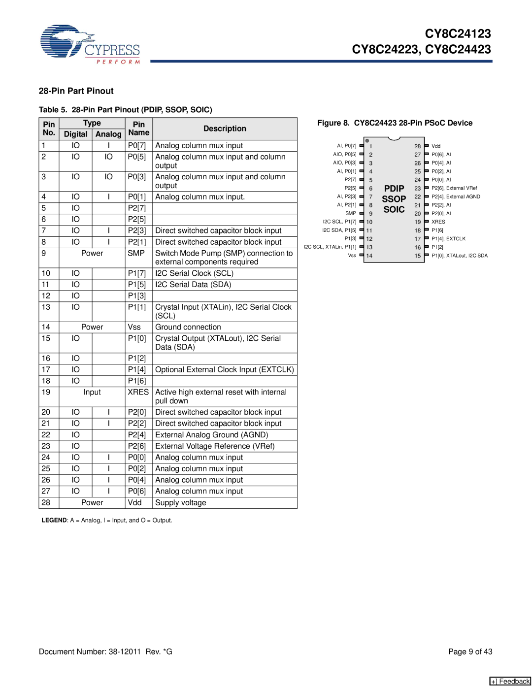
Table 5. 28-Pin Part Pinout (PDIP, SSOP, SOIC)

Pin

Type

Pin

Description

No.

Digital Analog

Name


Figure 8. CY8C24423 28-Pin PSoC Device

1

IO


I

P0[7]

Analog column mux input

2

IO


IO

P0[5]

Analog column mux input and column


output

3

IO


IO

P0[3]

Analog column mux input and column


output

4

IO


I

P0[1]

Analog column mux input.

5

IO


P2[7]


6

IO


P2[5]


7

IO


I

P2[3]

Direct switched capacitor block input

8

IO


I

P2[1]

Direct switched capacitor block input

9


Power

SMP

Switch Mode Pump (SMP) connection to


external components required

10

IO


P1[7]

I2C Serial Clock (SCL)

11

IO


P1[5]

I2C Serial Data (SDA)

12

IO


P1[3]


13

IO


P1[1]

Crystal Input (XTALin), I2C Serial Clock


(SCL)

14


Power

Vss

Ground connection

15

IO


P1[0]

Crystal Output (XTALout), I2C Serial


Data (SDA)

16

IO


P1[2]


17

IO


P1[4]

Optional External Clock Input (EXTCLK)

18

IO


P1[6]


19


Input

XRES

Active high external reset with internal


pull down

20

IO


I

P2[0]

Direct switched capacitor block input

21

IO


I

P2[2]

Direct switched capacitor block input

22

IO


P2[4]

External Analog Ground (AGND)

23

IO


P2[6]

External Voltage Reference (VRef)

24

IO


I

P0[0]

Analog column mux input

25

IO


I

P0[2]

Analog column mux input

26

IO


I

P0[4]

Analog column mux input

27

IO


I

P0[6]

Analog column mux input

28


Power

Vdd

Supply voltage

LEGEND: A = Analog, I = Input, and O = Output.

AI, P0[7]


1


28


AIO, P0[5]


2


27


AIO, P0[3]


3


26


AI, P0[1]


4


25


P2[7]


5

PDIP

24


P2[5]


6

23


AI, P2[3]


7

SSOP

22


AI, P2[1]


8

SOIC

21


SMP


9

20


I2C SCL, P1[7]


10


19


I2C SDA, P1[5]


11


18


P1[3]


12


17


I2C SCL, XTALin, P1[1]


13


16


Vss


14


15


Vdd P0[6], AI P0[4], AI P0[2], AI P0[0], AI

P2[6], External VRef P2[4], External AGND P2[2], AI

P2[0], AI XRES P1[6]

P1[4], EXTCLK P1[2]

P1[0], XTALout, I2C SDA

Document Number: 38-12011 Rev. *G

Page 9 of 43

[+] Feedback

Page 9
Image 9
Cypress CY8C24123, CY8C24223, CY8C24423 Switch Mode Pump SMP connection to, External components required, Scl, Pull down

CY8C24123, CY8C24423, CY8C24223 specifications

The Cypress CY8C24223, CY8C24423, and CY8C24123 are members of the PSoC (Programmable System-on-Chip) family, which combine a microcontroller with configurable analog and digital blocks. These devices are designed for a variety of embedded applications, offering versatility and performance for developers looking to create custom solutions.

One of the standout features of the CY8C24223, CY8C24423, and CY8C24123 is their programmable analog and digital components. These include operational amplifiers, comparators, and even CapSense technology, enabling touch sensing capabilities. This flexibility allows engineers to configure the chip according to the specific needs of their application, thereby reducing the number of external components required and simplifying PCB design.

The microcontroller core in these PSoC devices is a 16-bit architecture, offering a balance between performance and power efficiency. The CY8C24223 and CY8C24423 variants include higher RAM and Flash memory options, catering to more demanding applications compared to the CY8C24123. This makes them suitable for tasks ranging from simple control operations to more complex computational processes.

A key technology utilized in these devices is the integrated programmable interconnect, which allows for easy communication between the various configurable blocks. This feature significantly speeds up the development process by enabling designers to create custom peripheral setups without the need for extensive coding.

In addition to their hardware features, Cypress provides an intuitive design environment called PSoC Creator. This IDE simplifies the process of configuring the device, allowing developers to drag and drop components into a design schematic and generate code effortlessly. PSoC Creator also includes simulation features, enabling testing and validation of designs before deployment.

The PSoC family is known for its low power consumption, which is crucial for battery-operated devices. The power management features integrated into these models allow for various operational modes, making them energy-efficient and ideal for portable applications.

In summary, the Cypress CY8C24223, CY8C24423, and CY8C24123 are powerful and flexible programmable system-on-chip solutions. With a combination of configurable analog and digital blocks, solid performance specifications, and an easy-to-use development environment, these devices stand out for engineers working on innovative embedded applications across numerous industries. Their low power consumption further enhances their appeal for modern applications, making them a strong choice for designers.