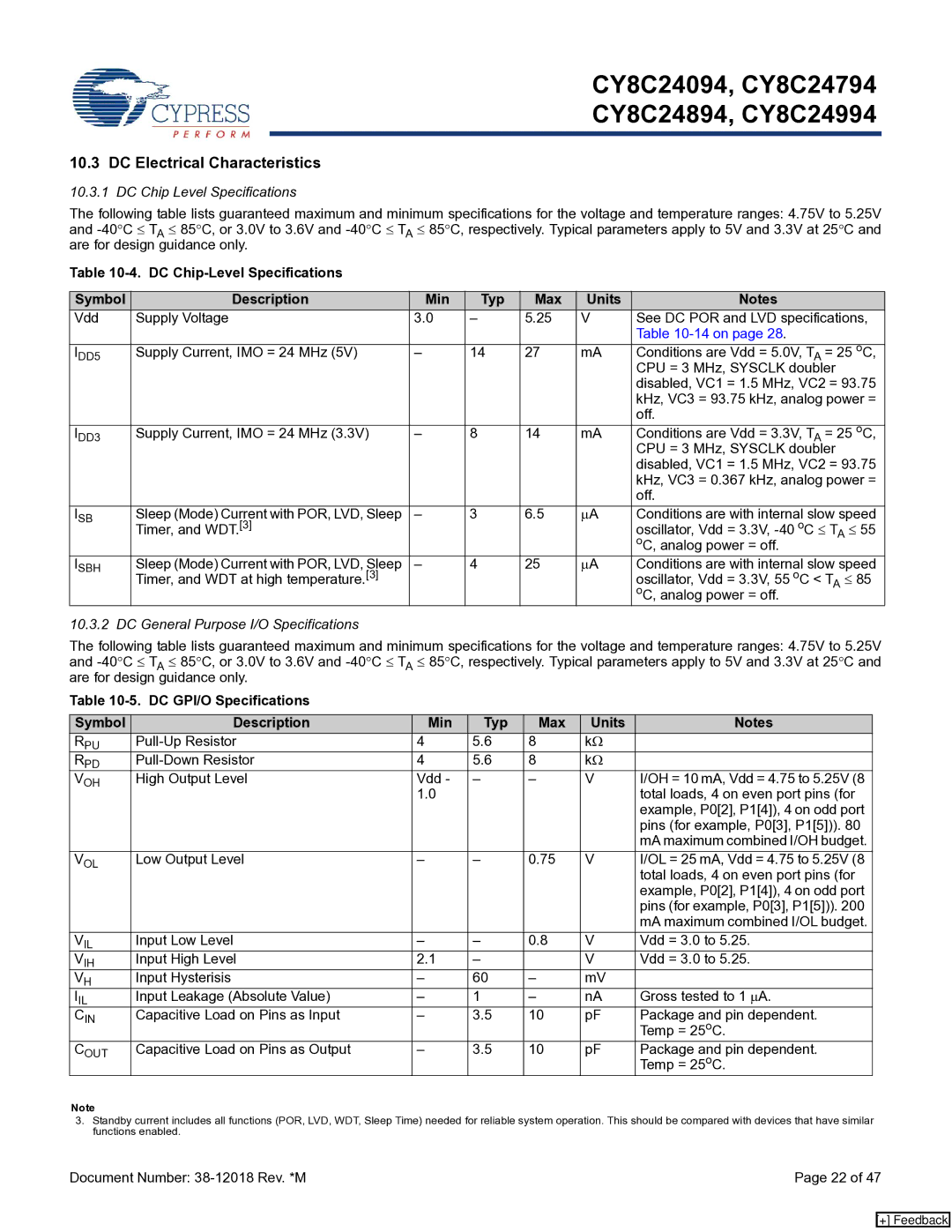
CY8C24094, CY8C24894, CY8C24994 specifications
The Cypress CY8C24994, CY8C24894, and CY8C24094 are part of the PSoC (Cypress Semiconductor's Programmable System-on-Chip) family, designed to integrate numerous functions onto a single chip for efficient performance and flexibility in various applications.One of the key features of these devices is their combination of analog and digital components, allowing designers to create a customized system without the need for extensive external circuitry. Each of these chips incorporates an Arm Cortex-M3 processor core, which provides a powerful 32-bit architecture, enabling efficient execution of 32-bit operations while maintaining low power consumption.
The CY8C24994 is the most advanced in this series, supporting up to 128 GPIO (General Purpose Input/Output) pins, which enhances connectivity options. It features multiple programmable analog blocks, including op-amps, comparators, and DACs (Digital-to-Analog Converters), making it suitable for a variety of sensor interfacing and signal processing applications. Additionally, it supports USB communication, providing further versatility for applications requiring data exchange with a host device.
The CY8C24894 presents a slightly more cost-effective solution with slightly fewer GPIO pins and integrated features. It maintains many of the same core attributes as its counterpart, delivering excellent analog performance and several programmable digital blocks. It is suitable for applications requiring moderate computational capabilities along with flexibility in terms of peripherals and interfaces.
The CY8C24094, while positioned as a more basic option within this lineup, still provides essential functionalities for simpler tasks. With fewer pins and capabilities, it is ideal for applications where size and cost are more critical than extensive processing power.
All three devices utilize Cypress's proprietary CapSense technology, enabling touch-sensing capabilities without the need for mechanical buttons. This feature not only enhances user interaction but also contributes to the overall design's robustness and longevity.
In summary, the CY8C24994, CY8C24894, and CY8C24094 PSoC chips offer ample design flexibility with integrated analog and digital functionality, making them an excellent choice for developers aiming to create innovative embedded solutions across a wide range of applications, from consumer electronics to industrial control systems.

