STK14CA8
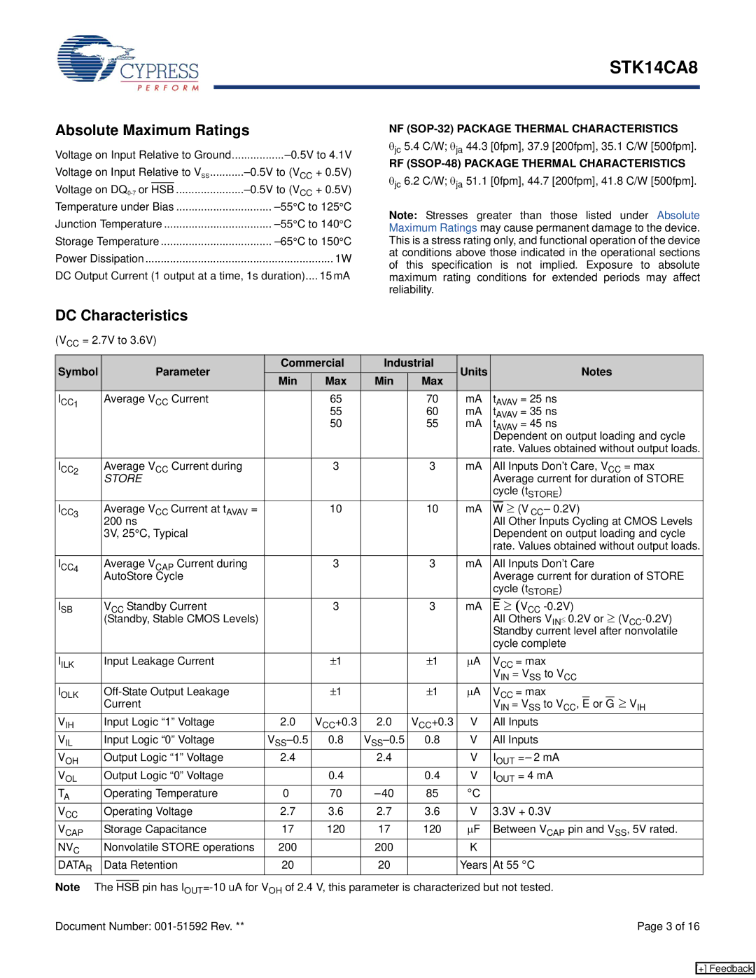
Absolute Maximum Ratings
Voltage on Input Relative to Ground | |||
Voltage on Input Relative to VSS | |||
Voltage on | HSB | ...................... | |
Temperature under Bias | |||
Junction Temperature | |||
Storage Temperature | |||
Power Dissipation | 1W | ||
DC Output Current (1 output at a time, 1s duration).... 15 mA
NF
θjc 5.4 C/W; θja 44.3 [0fpm], 37.9 [200fpm], 35.1 C/W [500fpm].
RF
θjc 6.2 C/W; θja 51.1 [0fpm], 44.7 [200fpm], 41.8 C/W [500fpm].
Note: Stresses greater than those listed under Absolute Maximum Ratings may cause permanent damage to the device. This is a stress rating only, and functional operation of the device at conditions above those indicated in the operational sections of this specification is not implied. Exposure to absolute maximum rating conditions for extended periods may affect reliability.
DC Characteristics
(VCC = 2.7V to 3.6V)
Symbol |
|
| Parameter | Commercial | Industrial | Units |
|
|
|
|
|
|
| Notes |
| ||||||
|
| Min | Max | Min | Max |
|
|
|
|
|
|
|
| ||||||||
|
|
|
|
|
|
|
|
|
|
|
|
|
|
|
|
|
| ||||
ICC1 | Average VCC Current |
| 65 |
| 70 | mA |
| tAVAV | = 25 ns |
| |||||||||||
|
|
|
|
| 55 |
| 60 | mA |
| tAVAV | = 35 ns |
| |||||||||
|
|
|
|
| 50 |
| 55 | mA |
| tAVAV | = 45 ns |
| |||||||||
|
|
|
|
|
|
|
|
|
| Dependent on output loading and cycle | |||||||||||
|
|
|
|
|
|
|
|
|
| rate. Values obtained without output loads. | |||||||||||
ICC2 | Average VCC Current during |
| 3 |
| 3 | mA | All Inputs Don’t Care, VCC = max | ||||||||||||||
| STORE |
|
|
|
|
|
| Average current for duration of STORE | |||||||||||||
|
|
|
|
|
|
|
|
|
| cycle (tSTORE) |
| ||||||||||
ICC3 | Average VCC Current at tAVAV = |
| 10 |
| 10 | mA |
| W | ≥ (V CC– 0.2V) |
| |||||||||||
| 200 ns |
|
|
|
|
|
| All Other Inputs Cycling at CMOS Levels | |||||||||||||
| 3V, 25°C, Typical |
|
|
|
|
|
| Dependent on output loading and cycle | |||||||||||||
|
|
|
|
|
|
|
|
|
| rate. Values obtained without output loads. | |||||||||||
ICC4 | Average VCAP Current during |
| 3 |
| 3 | mA | All Inputs Don’t Care |
| |||||||||||||
| AutoStore Cycle |
|
|
|
|
|
| Average current for duration of STORE | |||||||||||||
|
|
|
|
|
|
|
|
|
| cycle (tSTORE) |
| ||||||||||
ISB | VCC Standby Current |
| 3 |
| 3 | mA |
| E | ≥ (VCC |
| |||||||||||
| (Standby, Stable CMOS Levels) |
|
|
|
|
|
| All Others VIN≤ 0.2V or ≥ | |||||||||||||
|
|
|
|
|
|
|
|
|
| Standby current level after nonvolatile | |||||||||||
|
|
|
|
|
|
|
|
|
| cycle complete |
| ||||||||||
IILK | Input Leakage Current |
| ±1 |
| ±1 | μA |
| VCC | = max |
| |||||||||||
|
|
|
|
|
|
|
|
|
| VIN = VSS to VCC |
| ||||||||||
I |
| ±1 |
| ±1 | μA |
| V | = max |
| ||||||||||||
OLK | Current |
|
|
|
|
|
| VCC= V |
| to V , |
| or |
| ≥ V |
| ||||||
|
|
|
|
|
| SS | E | G | IH | ||||||||||||
|
|
|
|
|
|
|
|
|
|
| IN |
|
| CC | |||||||
VIH | Input Logic “1” Voltage | 2.0 | VCC+0.3 | 2.0 | VCC+0.3 | V |
| All Inputs |
|
|
|
|
|
| |||||||
VIL | Input Logic “0” Voltage | 0.8 | 0.8 | V | All Inputs |
|
|
|
|
|
| ||||||||||
VOH | Output Logic “1” Voltage | 2.4 |
| 2.4 |
| V |
| IOUT = – 2 mA |
| ||||||||||||
VOL | Output Logic “0” Voltage |
| 0.4 |
| 0.4 | V |
| IOUT = 4 mA |
| ||||||||||||
TA | Operating Temperature | 0 | 70 | 85 | °C |
|
|
|
|
|
|
|
|
|
|
|
|
| |||
VCC | Operating Voltage | 2.7 | 3.6 | 2.7 | 3.6 | V | 3.3V + 0.3V |
| |||||||||||||
VCAP | Storage Capacitance | 17 | 120 | 17 | 120 | μF |
| Between VCAP pin and VSS, 5V rated. | |||||||||||||
NVC | Nonvolatile STORE operations | 200 |
| 200 |
| K |
|
|
|
|
|
|
|
|
|
|
|
|
| ||
DATAR | Data Retention | 20 |
| 20 |
| Years | At 55 °C |
|
|
|
|
|
| ||||||||
Note The |
| pin has |
| ||||||||||||||||||
HSB |
| ||||||||||||||||||||
Document Number: |
|
|
|
|
|
|
|
|
|
|
|
|
|
|
|
|
| Page 3 of 16 | |||
[+] Feedback