STK15C88
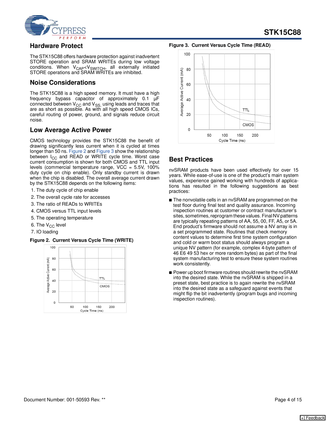
Hardware Protect | Figure 3. Current Versus Cycle Time (READ) |
The STK15C88 offers hardware protection against inadvertent STORE operation and SRAM WRITEs during low voltage conditions. When VCAP<VSWITCH, all externally initiated STORE operations and SRAM WRITEs are inhibited.
Noise Considerations
The STK15C88 is a high speed memory. It must have a high frequency bypass capacitor of approximately 0.1 µF connected between VCC and VSS, using leads and traces that are as short as possible. As with all high speed CMOS ICs, careful routing of power, ground, and signals reduce circuit noise.
Low Average Active Power
CMOS technology provides the STK15C88 the benefit of drawing significantly less current when it is cycled at times longer than 50 ns. Figure 2 and Figure 3 show the relationship between ICC and READ or WRITE cycle time. Worst case current consumption is shown for both CMOS and TTL input levels (commercial temperature range, VCC = 5.5V, 100% duty cycle on chip enable). Only standby current is drawn when the chip is disabled. The overall average current drawn by the STK15C88 depends on the following items:
1.The duty cycle of chip enable
2.The overall cycle rate for accesses
3.The ratio of READs to WRITEs
4.CMOS versus TTL input levels
5.The operating temperature
6.The VCC level
7.IO loading
Figure 2. Current Versus Cycle Time (WRITE)
Best Practices
nvSRAM products have been used effectively for over 15 years. While
■The nonvolatile cells in an nvSRAM are programmed on the test floor during final test and quality assurance. Incoming inspection routines at customer or contract manufacturer’s sites, sometimes, reprogram these values. Final NV patterns are typically repeating patterns of AA, 55, 00, FF, A5, or 5A. End product’s firmware should not assume a NV array is in a set programmed state. Routines that check memory content values to determine first time system configuration and cold or warm boot status should always program a unique NV pattern (for example, complex
■Power up boot firmware routines should rewrite the nvSRAM into the desired state. While the nvSRAM is shipped in a preset state, best practice is to again rewrite the nvSRAM into the desired state as a safeguard against events that might flip the bit inadvertently (program bugs and incoming inspection routines).
Document Number: | Page 4 of 15 |
[+] Feedback