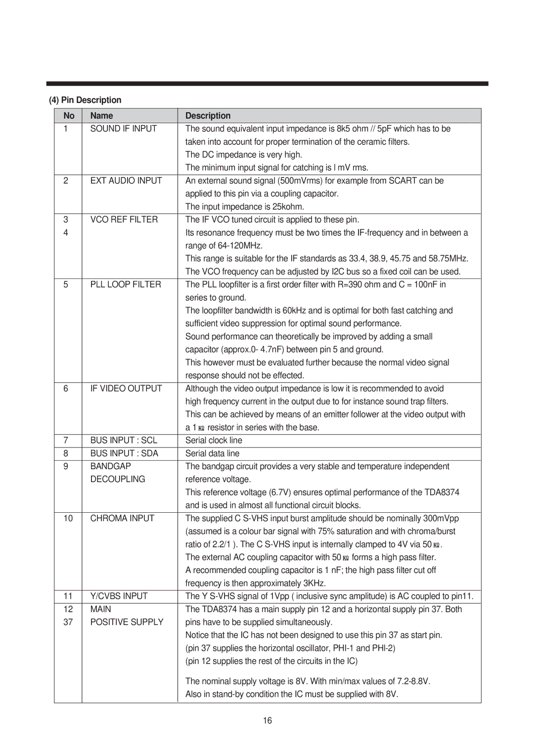
(4) Pin Description
No | Name | Description |
|
|
|
1 | SOUND IF INPUT | The sound equivalent input impedance is 8k5 ohm // 5pF which has to be |
|
| taken into account for proper termination of the ceramic filters. |
|
| The DC impedance is very high. |
|
| The minimum input signal for catching is l mV rms. |
|
|
|
2 | EXT AUDIO INPUT | An external sound signal (500mVrms) for example from SCART can be |
|
| applied to this pin via a coupling capacitor. |
|
| The input impedance is 25kohm. |
|
|
|
3 | VCO REF FILTER | The IF VCO tuned circuit is applied to these pin. |
4 |
| Its resonance frequency must be two times the |
|
| range of |
|
| This range is suitable for the IF standards as 33.4, 38.9, 45.75 and 58.75MHz. |
|
| The VCO frequency can be adjusted by I2C bus so a fixed coil can be used. |
|
|
|
5 | PLL LOOP FILTER | The PLL loopfilter is a first order filter with R=390 ohm and C = 100nF in |
|
| series to ground. |
|
| The loopfilter bandwidth is 60kHz and is optimal for both fast catching and |
|
| sufficient video suppression for optimal sound performance. |
|
| Sound performance can theoretically be improved by adding a small |
|
| capacitor (approx.0- 4.7nF) between pin 5 and ground. |
|
| This however must be evaluated further because the normal video signal |
|
| response should not be effected. |
|
|
|
6 | IF VIDEO OUTPUT | Although the video output impedance is low it is recommended to avoid |
|
| high frequency current in the output due to for instance sound trap filters. |
|
| This can be achieved by means of an emitter follower at the video output with |
|
| a 1 resistor in series with the base. |
|
|
|
7 | BUS INPUT : SCL | Serial clock line |
|
|
|
8 | BUS INPUT : SDA | Serial data line |
|
|
|
9 | BANDGAP | The bandgap circuit provides a very stable and temperature independent |
| DECOUPLING | reference voltage. |
|
| This reference voltage (6.7V) ensures optimal performance of the TDA8374 |
|
| and is used in almost all functional circuit blocks. |
|
|
|
10 | CHROMA INPUT | The supplied C |
|
| (assumed is a colour bar signal with 75% saturation and with chroma/burst |
|
| ratio of 2.2/1 ). The C |
|
| The external AC coupling capacitor with 50 forms a high pass filter. |
|
| A recommended coupling capacitor is 1 nF; the high pass filter cut off |
|
| frequency is then approximately 3KHz. |
|
|
|
11 | Y/CVBS INPUT | The Y |
|
|
|
12 | MAIN | The TDA8374 has a main supply pin 12 and a horizontal supply pin 37. Both |
37 | POSITIVE SUPPLY | pins have to be supplied simultaneously. |
|
| Notice that the IC has not been designed to use this pin 37 as start pin. |
|
| (pin 37 supplies the horizontal oscillator, |
|
| (pin 12 supplies the rest of the circuits in the IC) |
|
| The nominal supply voltage is 8V. With min/max values of |
|
| Also in |
|
|
|
16
