TDA4665(Base Band Delay Line)
(1)Features
•Two comb filters, using the
•Adjustment free application
•No crosstalk between SECAM colour carriers
•Handles negative or positive
•Clamping of
•VCO without external components
•3MHz internal clock signal derived from a 6MHz VCO,
•
•Addition of delayed and
•Output buffer amplifiers
•Comb filtering functions for NTSC
(2)General Description
The TDA4661 is an integrated baseband delay line circuit with one line delay. It is suitable for decoders with
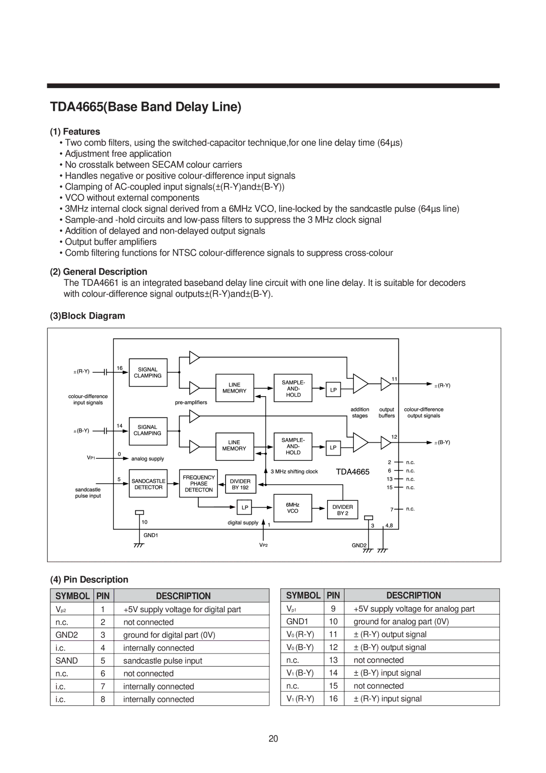
(3)Block Diagram
(4) Pin Description
SYMBOL | PIN | DESCRIPTION |
Vp2 | 1 | +5V supply voltage for digital part |
n.c. | 2 | not connected |
GND2 | 3 | ground for digital part (0V) |
i.c. | 4 | internally connected |
SAND | 5 | sandcastle pulse input |
n.c. | 6 | not connected |
i.c. | 7 | internally connected |
i.c. | 8 | internally connected |
|
|
|
|
|
|
|
|
|
|
|
|
|
|
|
|
|
|
|
|
|
|
|
|
|
|
|
|
|
|
|
|
|
|
|
|
|
|
|
|
|
|
|
|
|
|
|
|
|
|
|
|
|
|
|
|
|
|
|
|
|
|
|
|
|
|
|
|
|
|
|
|
|
|
|
|
|
|
|
|
|
|
|
|
|
|
|
|
|
|
|
|
|
|
|
|
|
|
|
|
|
|
|
|
|
|
|
|
|
|
|
|
|
|
|
|
|
|
|
|
|
|
|
|
|
|
|
|
|
|
|
|
|
|
|
|
|
|
|
|
|
|
|
|
|
|
|
|
|
|
|
|
|
|
|
|
|
|
|
|
|
|
|
|
|
|
|
|
|
|
|
|
|
|
|
|
|
|
|
|
|
|
|
|
|
|
|
|
|
|
|
|
|
|
|
|
|
|
|
|
|
|
|
|
|
|
|
|
|
|
|
|
|
|
|
|
|
|
|
|
|
|
|
|
|
|
|
|
|
|
|
|
|
|
|
|
|
|
|
|
|
|
|
|
|
|
|
|
|
|
|
|
|
|
|
|
|
|
|
|
|
|
|
|
|
|
|
|
|
|
|
|
|
|
|
|
|
|
|
|
|
|
|
|
|
|
|
|
|
|
|
|
|
|
|
|
|
|
|
|
|
|
|
|
|
|
|
|
|
|
|
|
|
|
|
|
|
|
| SYMBOL |
| PIN |
|
|
|
| DESCRIPTION | ||||||
| Vp1 |
| 9 |
| +5V supply voltage for analog part | |||||||||
| GND1 |
| 10 |
| ground for analog part (0V) | |||||||||
| V0 |
| 11 |
| ± | |||||||||
| V0 |
| 12 |
| ± | |||||||||
| n.c. |
| 13 |
| not connected | |||||||||
| V1 |
| 14 |
| ± | |||||||||
| n.c. |
| 15 |
| not connected | |||||||||
| V1 |
| 16 |
| ± | |||||||||
|
|
|
|
|
|
|
|
|
|
|
|
|
|
|
20