11.3 Register Bit Definitions

In these register definitions, a bit marked ‘X’ is an unused bit.

All unused bits in readable registers read back as 0.

Base + 0

Write

Command Register


Bit No.

7

6

5

4

3

2

1

0


Name

STRTAD

RSTBRD

RSTDA

RSTFIFO

CLRDMA

CLRT

CLRD

CLRA


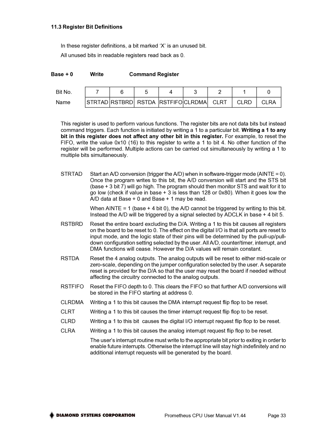
This register is used to perform various functions. The register bits are not data bits but instead command triggers. Each function is initiated by writing a 1 to a particular bit. Writing a 1 to any bit in this register does not affect any other bit in this register. For example, to reset the FIFO, write the value 0x10 (16) to this register to write a 1 to bit 4. No other function of the register will be performed. Multiple actions can be carried out simultaneously by writing a 1 to multiple bits simultaneously.

STRTAD

Start an A/D conversion (trigger the A/D) when in software-trigger mode (AINTE = 0).


Once the program writes to this bit, the A/D conversion will start and the STS bit


(base + 3 bit 7) will go high. The program should then monitor STS and wait for it to


go low (check if value in base + 3 is less than 128 or 0x80). When it goes low the


A/D data at Base + 0 and Base + 1 may be read.


When AINTE = 1 (base + 4 bit 0), the A/D cannot be triggered by writing to this bit.


Instead the A/D will be triggered by a signal selected by ADCLK in base + 4 bit 5.

RSTBRD

Reset the entire board excluding the D/A. Writing a 1 to this bit causes all registers


on the board to be reset to 0. The effect on the digital I/O is that all ports are reset to


input mode, and the logic state of their pins will be determined by the pull-up/pull-


down configuration setting selected by the user. All A/D, counter/timer, interrupt, and


DMA functions will cease. However the D/A values will remain constant.

RSTDA

Reset the 4 analog outputs. The analog outputs will be reset to either mid-scale or


zero-scale, depending on the jumper configuration selected by the user. A separate


reset is provided for the D/A so that the user may reset the board if needed without


affecting the circuitry connected to the analog outputs.

RSTFIFO

Reset the FIFO depth to 0. This clears the FIFO so that further A/D conversions will


be stored in the FIFO starting at address 0.

CLRDMA

Writing a 1 to this bit causes the DMA interrupt request flip flop to be reset.

CLRT

Writing a 1 to this bit causes the timer interrupt request flip flop to be reset.

CLRD

Writing a 1 to this bit causes the digital I/O interrupt request flip flop to be reset.

CLRA

Writing a 1 to this bit causes the analog interrupt request flip flop to be reset.


The user’s interrupt routine must write to the appropriate bit prior to exiting in order to


enable future interrupts. Otherwise the interrupt line will stay high indefinitely and no


additional interrupt requests will be generated by the board.

Prometheus CPU User Manual V1.44

Page 33

Page 33
Image 33
Diamond Systems PR-Z32-E-ST, PR-Z32-EA-ST user manual Register Bit Definitions, Base +, Command Register

PR-Z32-E-ST, PR-Z32-EA-ST specifications

The Diamond Systems PR-Z32-EA-ST and PR-Z32-E-ST are pioneering solutions in the realm of embedded computing systems, designed to meet the challenging demands of various industrial applications. These boards harness advanced technologies and a comprehensive feature set to ensure exceptional performance, flexibility, and reliability.

At the heart of the PR-Z32 series is a robust processor architecture that combines efficiency with processing power. The systems are built around the Zynq-7000 SoC (System on Chip), which integrates a dual-core ARM Cortex-A9 processor with Xilinx FPGA technology. This hybrid architecture provides the ability to run complex algorithms and custom logic concurrently, making the boards ideal for applications requiring intense computational tasks such as image processing, data acquisition, and real-time control.

One of the main features of the PR-Z32-EA-ST and PR-Z32-E-ST is their versatility. Both variants support a wide range of I/O options, including USB, Ethernet, CAN, and serial interfaces. This range of connectivity allows for integrations with various sensors, actuators, and other peripheral devices, making it suitable for industrial automation, robotics, and IoT projects. The inclusion of multiple GPIO pins also enhances the capability of the boards to interface with additional hardware.

In terms of performance, the PR-Z32 series supports substantial amounts of on-board memory, which can be essential for applications requiring the storage and processing of large datasets. The configurations are often customizable, allowing users to select the appropriate amount of RAM and on-board flash memory for their specific applications.

Reliability is a critical characteristic of the Diamond Systems PR-Z32 series. The boards are built to withstand adverse environmental conditions, making them suitable for deployment in industrial environments. They are often designed to operate over a wide temperature range, ensuring functionality in both hot and cold climates. Additionally, the boards are compliant with various industry standards, assuring users of their robustness and durability.

Moreover, the PR-Z32-EA-ST and PR-Z32-E-ST support real-time operating systems (RTOS) and conventional operating systems such as Linux. This support provides developers with the flexibility to choose the best environment for their applications, whether they require real-time performance or full-fledged operating system features.

In conclusion, the Diamond Systems PR-Z32-EA-ST and PR-Z32-E-ST are formidable options for those seeking powerful, versatile, and reliable embedded computing solutions. With their advanced SoC architecture, flexible I/O options, extensive memory configurations, and environmental resilience, these boards are well-equipped to tackle the challenges of modern industrial applications.