FMV156DBE specifications
The Electrolux FMV156DBE is a modern and versatile microwave oven that combines sleek aesthetics with cutting-edge technology, making it a popular choice for contemporary kitchens. This model offers a range of advanced features designed to streamline cooking and enhance convenience while ensuring users can prepare meals efficiently.One of the standout features of the Electrolux FMV156DBE is its powerful 1.6 cubic feet capacity, which provides ample space for cooking various dishes, from reheating leftovers to defrosting frozen goods. Its 1,000-watt power output allows for fast and efficient cooking, ensuring that food is heated evenly and thoroughly. The microwave also features multiple power levels, enabling users to customize cooking intensity based on their specific needs.
This model is equipped with the Sensor Cooking technology, which automatically adjusts cooking time and power based on the moisture released from the food. This intelligent feature helps to prevent overcooking or undercooking, delivering perfectly prepared meals every time. Additionally, the FMV156DBE includes a range of pre-programmed cooking settings that cater to different food types, further enhancing usability and efficiency.
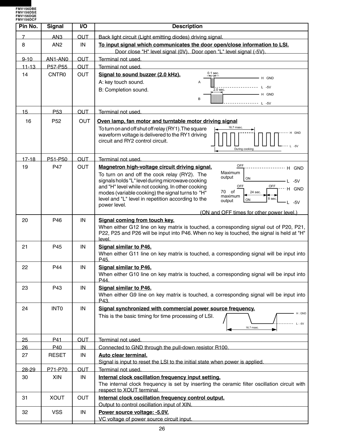
Another notable aspect of the Electrolux FMV156DBE is its intuitive touch control panel, allowing for easy navigation through cooking options and settings. The illuminated LED display enhances visibility, making it simple to monitor cooking progress at a glance. The microwave also features a convenient kitchen timer and a clock function, adding to its overall functionality.
The microwave not only excels in cooking performance but also in design. It features a contemporary stainless-steel finish that adds a touch of elegance to any kitchen decor. The streamlined design ensures it can fit seamlessly into various kitchen layouts, while the built-in design options provide flexibility for installation.
Safety is also a priority with the Electrolux FMV156DBE, which includes a child lock feature, preventing unintended use by little hands. This quality makes it an ideal appliance for families with children.
In summary, the Electrolux FMV156DBE is a highly functional microwave oven that features advanced cooking technologies, an ample cooking capacity, and a stylish design. With its combination of performance, convenience, and safety features, it serves as a valuable addition to any modern kitchen.

