14 | |||
|
|
|
|
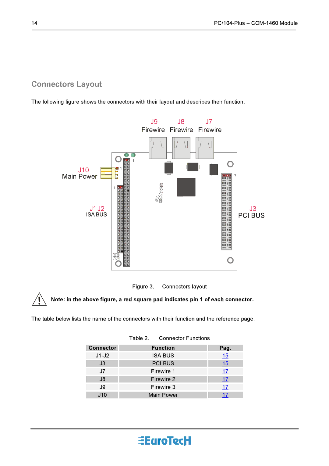
Connectors Layout
The following figure shows the connectors with their layout and describes their function.
J9 J8 J7
Firewire Firewire Firewire
J10 |
|
Main Power |
|
J1 J2 | J3 |
| PCI BUS |
Figure 3. Connectors layout
Note: in the above figure, a red square pad indicates pin 1 of each connector.
The table below lists the name of the connectors with their function and the reference page.
Table 2. Connector Functions
|
| Connector |
| Function |
| Pag. |
|
|
|
|
|
|
|
|
|
|
|
|
|
| ISA BUS |
| 15 |
|
| |
|
|
|
|
|
|
|
|
|
|
| J3 |
| PCI BUS |
| 15 |
|
|
|
|
|
|
|
|
|
|
|
|
| J7 |
| Firewire 1 |
| 17 |
|
|
|
|
|
|
|
|
|
|
|
|
| J8 |
| Firewire 2 |
| 17 |
|
|
|
|
|
|
|
|
|
|
|
|
| J9 |
| Firewire 3 |
| 17 |
|
|
|
|
|
|
|
|
|
|
|
|
| J10 |
| Main Power |
| 17 |
|
|
|
|
|
|
|
|
|
|
|