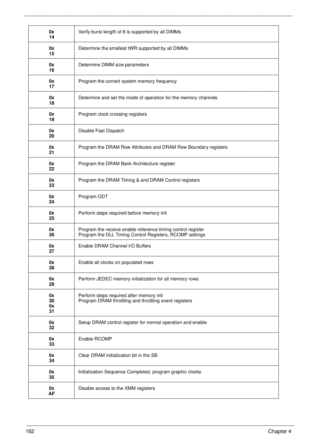
0x | Verify burst length of 8 is supported by all DIMMs |
14 |
|
|
|
0x | Determine the smallest tWR supported by all DIMMs |
15 |
|
|
|
0x | Determine DIMM size parameters |
16 |
|
|
|
0x | Program the correct system memory frequency |
17 |
|
|
|
0x | Determine and set the mode of operation for the memory channels |
18 |
|
|
|
0x | Program clock crossing registers |
19 |
|
|
|
0x | Disable Fast Dispatch |
20 |
|
|
|
0x | Program the DRAM Row Attributes and DRAM Row Boundary registers |
21 |
|
0x | Program the DRAM Bank Architecture register |
22 |
|
|
|
0x | Program the DRAM Timing & and DRAM Control registers |
23 |
|
|
|
0x | Program ODT |
24 |
|
|
|
0x | Perform steps required before memory init |
25 |
|
|
|
0x | Program the receive enable reference timing control register |
26 | Program the DLL Timing Control Registers, RCOMP settings |
|
|
0x | Enable DRAM Channel I/O Buffers |
27 |
|
|
|
0x | Enable all clocks on populated rows |
28 |
|
|
|
0x | Perform JEDEC memory initialization for all memory rows |
29 |
|
|
|
0x | Perform steps required after memory init |
30 | Program DRAM throttling and throttling event registers |
0x |
|
31 |
|
|
|
0x | Setup DRAM control register for normal operation and enable |
32 |
|
|
|
0x | Enable RCOMP |
33 |
|
|
|
0x | Clear DRAM initialization bit in the SB |
34 |
|
|
|
0x | Initialization Sequence Completed, program graphic clocks |
35 |
|
|
|
0x | Disable access to the XMM registers |
AF |
|
162 | Chapter 4 |
