3 |
Example: The analog output for a digital input of 0A00H would be:
1.0A00H decimal equivalent is 2560
2.Analog out =
=
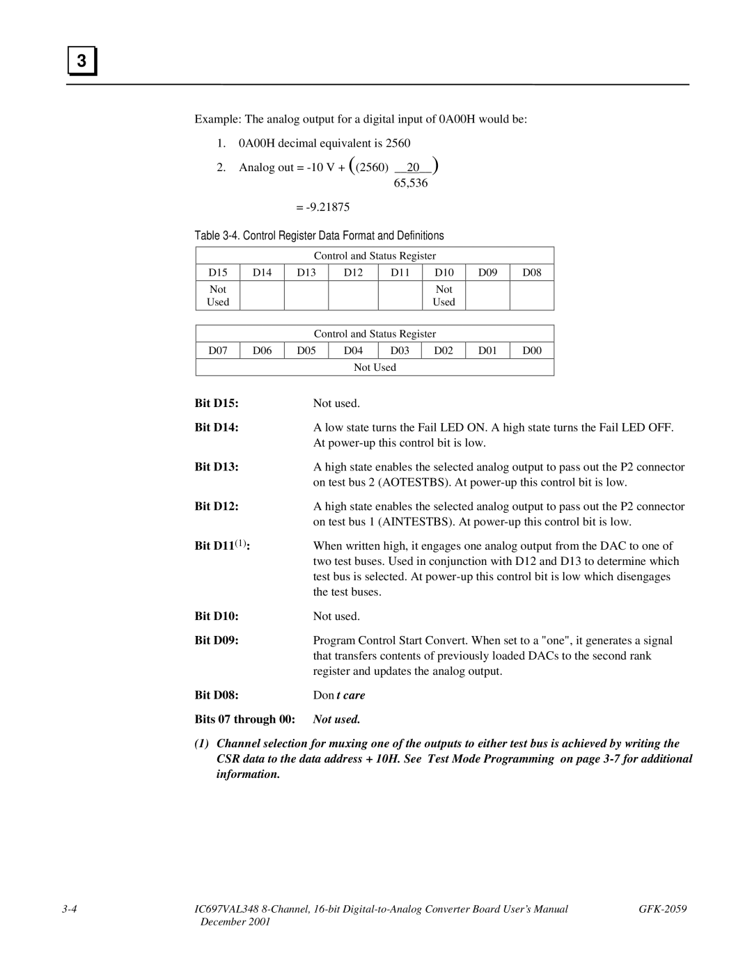
Table 3-4. Control Register Data Format and Definitions
D15
Not
Used
D14
Control and Status Register
D13 D12 D11 D10
Not
Used
D09
D08
D07
D06
Control and Status Register
D05 D04 D03 D02
Not Used
D01
D00
Bit D15: | Not used. |
Bit D14: | A low state turns the Fail LED ON. A high state turns the Fail LED OFF. |
| At |
Bit D13: | A high state enables the selected analog output to pass out the P2 connector |
| on test bus 2 (AOTESTBS). At |
Bit D12: | A high state enables the selected analog output to pass out the P2 connector |
| on test bus 1 (AINTESTBS). At |
Bit D11(1): | When written high, it engages one analog output from the DAC to one of |
| two test buses. Used in conjunction with D12 and D13 to determine which |
| test bus is selected. At |
| the test buses. |
Bit D10: | Not used. |
Bit D09: | Program Control Start Convert. When set to a "one", it generates a signal |
| that transfers contents of previously loaded DACs to the second rank |
| register and updates the analog output. |
Bit D08: | Don’t care |
Bits 07 through 00: | Not used. |
(1)Channel selection for muxing one of the outputs to either test bus is achieved by writing the CSR data to the data address + 10H. See “Test Mode Programming” on page
IC697VAL348 | ||
| – December 2001 |
|