CHAPTER 3 WIRING, CONNECTING
3.1 TERMINAL ASSIGNMENT OF DIGITAL INPUT OPTION BOARD
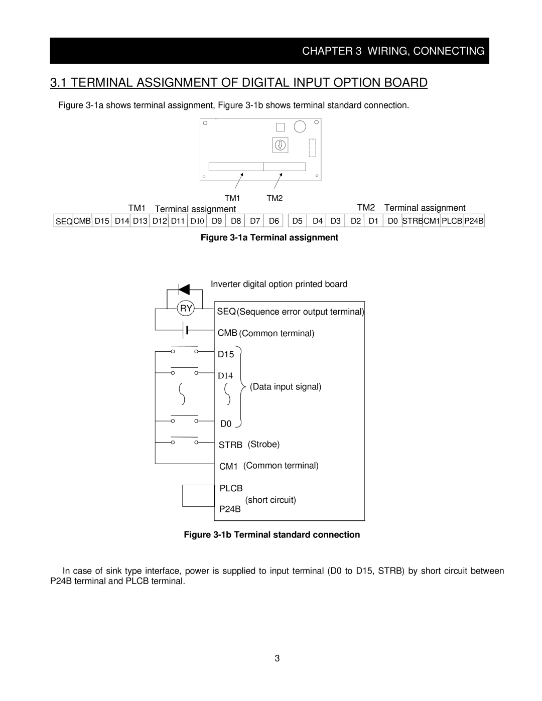
Figure 3-1a shows terminal assignment, Figure 3-1b shows terminal standard connection.
TM1 | TM2 |
TM1 Terminal assignment
SEQCMB ![]() D15 D14 D13 D12
D15 D14 D13 D12 ![]() D11
D11 ![]() D10 D9 D8
D10 D9 D8 ![]() D7 D6
D7 D6
TM2 Terminal assignment
D5 D4 D3 D2 ![]() D1 D0
D1 D0 ![]() STRBCM1 PLCB P24B
STRBCM1 PLCB P24B
Figure 3-1a Terminal assignment
Inverter digital option printed board
RY | SEQ(Sequence error output terminal) |
| |
| CMB (Common terminal) |
| D15 |
| D14 |
| (Data input signal) |
| D0 |
| STRB (Strobe) |
| CM1 (Common terminal) |
| PLCB |
| (short circuit) |
| P24B |
Figure 3-1b Terminal standard connection
In case of sink type interface, power is supplied to input terminal (D0 to D15, STRB) by short circuit between P24B terminal and PLCB terminal.
3