BIOS |
|
|
|
|
|
4-3 Advanced Chipset Features
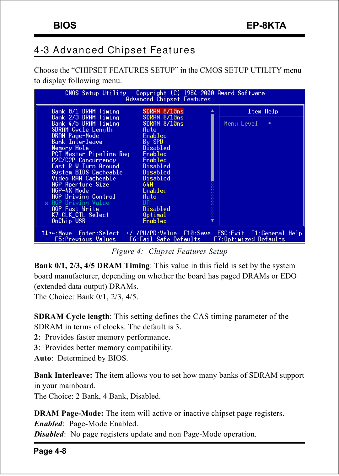
Choose the “CHIPSET FEATURES SETUP” in the CMOS SETUP UTILITY menu to display following menu.
Figure 4: Chipset Features Setup
Bank 0/1, 2/3, 4/5 DRAM Timing: This value in this field is set by the system board manufacturer, depending on whether the board has paged DRAMs or EDO (extended data output) DRAMs.
The Choice: Bank 0/1, 2/3, 4/5.
SDRAM Cycle length: This setting defines the CAS timing parameter of the SDRAM in terms of clocks. The default is 3.
2: Provides faster memory performance.
3: Provides better memory compatibility.
Auto: Determined by BIOS.
Bank Interleave: The item allows you to set how many banks of SDRAM support in your mainboard.
The Choice: 2 Bank, 4 Bank, Disabled.
DRAM Page-Mode: The item will active or inactive chipset page registers.
Enabled: Page-Mode Enabled.
Disabled: No page registers update and non Page-Mode operation.
Page