Appendix B. System address maps
Appendix | B. |
| System |
| address maps |
|
|
|
|
|
|
|
|
|
|
|
|
|
|
|
|
| |||||||
|
|
|
|
|
|
|
|
|
|
|
|
|
|
|
|
|
|
|
|
|
|
|
|
|
|
| |||
System |
| memory | map |
|
|
|
|
|
|
|
|
|
|
|
|
|
|
|
|
|
|
|
|
|
|
| |||
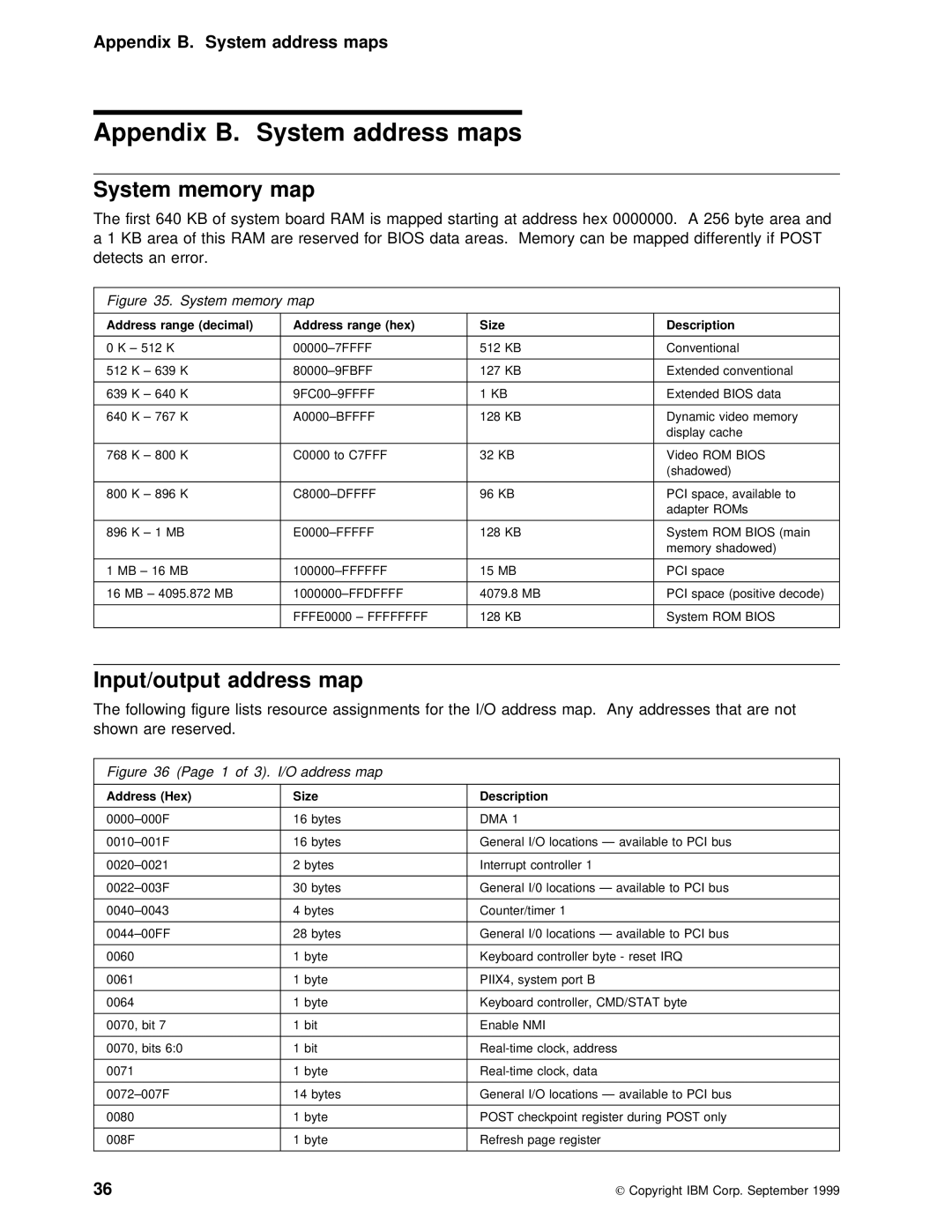
The | first | 640 | KB | of | system | board | RAM is | mapped | starting | at | address |
| hex 0000000. A 256 b | ||||||||||||||||
a 1 KB area of this RAM are reserved for | BIOS | data | areas. Memory | can | be mapped | ||||||||||||||||||||||||
detects | an | error. |
|
|
|
|
|
|
|
|
|
|
|
|
|
|
|
|
|
|
|
|
| ||||||
|
|
|
|
|
|
|
|
|
|
|
|
|
|
|
|
|
|
|
|
|
|
|
| ||||||
Figure | 35. |
| System memory map |
|
|
|
|
|
|
|
|
|
|
|
|
|
|
|
|
|
|
| |||||||
|
|
|
|
|
|
|
|
|
|
|
|
|
|
|
|
|
|
|
|
|
|
| |||||||
Address | range (decimal) |
|
|
| Address range | (hex) |
| Size |
|
|
|
|
|
| Description |
|
|
|
|
|
|
| |||||||
|
|
|
|
|
|
|
|
|
|
|
|
|
|
|
|
|
|
|
|
|
|
|
|
| |||||
0 K | – | 512 | K |
|
|
|
|
|
|
| 512 | KB |
|
|
|
|
| Conventional |
|
|
|
|
| ||||||
|
|
|
|
|
|
|
|
|
|
|
|
|
|
|
|
|
|
|
|
|
|
| |||||||
512 | K | – | 639 | K |
|
|
|
|
|
| 127 | KB |
|
|
|
|
| Extended | conventional |
|
| ||||||||
|
|
|
|
|
|
|
|
|
|
|
|
|
|
|
|
|
|
|
|
|
|
|
|
| |||||
639 | K | – | 640 | K |
|
|
|
|
|
|
| 1 | KB |
|
|
|
|
| Extended | BIOS | data |
|
| ||||||
|
|
|
|
|
|
|
|
|
|
|
|
|
|
|
|
|
|
|
|
|
|
|
|
|
| ||||
640 | K | – | 767 | K |
|
|
|
|
|
|
| 128 | KB |
|
|
|
|
| Dynamic |
| video | memory |
|
| |||||
|
|
|
|
|
|
|
|
|
|
|
|
|
|
|
|
|
|
|
|
| display |
| cache |
|
|
|
| ||
|
|
|
|
|
|
|
|
|
|
|
|
|
|
|
|
|
|
|
|
|
|
|
|
|
| ||||
768 | K | – | 800 | K |
|
|
|
| C0000 | to | C7FFF |
| 32 | KB |
|
|
|
|
| Video | ROM | BIOS |
|
|
| ||||
|
|
|
|
|
|
|
|
|
|
|
|
|
|
|
|
|
|
|
|
| (shadowed) |
|
|
|
|
| |||
|
|
|
|
|
|
|
|
|
|
|
|
|
|
|
|
|
|
|
|
|
|
|
| ||||||
800 | K | – | 896 | K |
|
|
|
|
|
|
| 96 KB |
|
|
|
|
| PCI | space, | available | to | ||||||||
|
|
|
|
|
|
|
|
|
|
|
|
|
|
|
|
|
|
|
|
| adapter | ROMs |
|
|
|
| |||
|
|
|
|
|
|
|
|
|
|
|
|
|
|
|
|
|
|
|
|
|
|
|
|
| |||||
896 | K | – | 1 MB |
|
|
|
|
|
|
| 128 | KB |
|
|
|
|
| System | ROM | BIOS | (main |
|
| ||||||
|
|
|
|
|
|
|
|
|
|
|
|
|
|
|
|
|
|
|
|
| memory | shadowed) |
|
|
| ||||
|
|
|
|
|
|
|
|
|
|
|
|
|
|
|
|
|
|
|
|
|
|
|
|
|
|
| |||
1 | MB | – | 16 | MB |
|
|
|
|
|
|
| 15 | MB |
|
|
|
|
| PCI | space |
|
|
|
|
| ||||
|
|
|
|
|
|
|
|
|
|
|
|
|
|
|
|
|
|
|
|
| |||||||||
16 | MB | – | 4095.872 | MB |
|
|
|
| 4079.8 MB |
|
|
|
|
| PCI | space | (positive | decode) | |||||||||||
|
|
|
|
|
|
|
|
|
|
|
|
|
|
|
|
|
|
|
|
|
|
|
|
| |||||
|
|
|
|
|
|
|
|
| FFFE0000 – | FFFFFFFF |
| 128 | KB |
|
|
|
|
| System | ROM | BIOS |
|
|
| |||||
|
|
|
|
|
|
|
|
|
|
|
|
|
|
|
|
|
|
|
|
|
|
|
| ||||||
|
|
|
|
|
|
|
|
|
|
|
|
|
|
|
|
|
|
|
|
|
|
|
|
|
|
|
|
|
|
Input/output | address |
| map |
|
|
|
|
|
|
|
|
|
|
|
|
|
|
|
|
|
|
|
| ||||||
The | following | figure | lists | resource | assignments | for |
| the | I/O | address | map. Any addresses | ||||||||||||||||||
shown | are | reserved. |
|
|
|
|
|
|
|
|
|
|
|
|
|
|
|
|
|
|
|
|
| ||||||
|
|
|
|
|
|
|
|
|
|
|
|
|
|
|
|
|
|
|
|
|
|
|
| ||||||
Figure | 36 | (Page | 1 |
| of | 3). |
| I/O address map |
|
|
|
|
|
|
|
|
|
|
|
|
|
|
| ||||||
|
|
|
|
|
|
|
|
|
|
|
|
|
|
|
|
|
|
|
|
|
|
|
|
|
|
| |||
Address | (Hex) |
|
|
|
|
| Size |
|
|
|
| Description |
|
|
|
|
|
|
|
|
|
|
|
|
|
| |||
|
|
|
|
|
|
|
|
|
|
|
|
|
|
|
|
|
|
|
|
|
|
|
|
|
|
|
| ||
|
|
|
|
|
|
| 16 | bytes |
|
| DMA | 1 |
|
|
|
|
|
|
|
|
|
|
|
|
|
| |||
|
|
|
|
|
|
|
|
|
|
|
|
|
| ||||||||||||||||
|
|
|
|
|
| 16 | bytes |
|
| General I/O locations — available to PCI bus |
|
| |||||||||||||||||
|
|
|
|
|
|
|
|
|
|
|
|
|
|
|
|
|
|
|
|
|
|
| |||||||
|
|
|
|
|
| 2 | bytes |
|
| Interrupt controller | 1 |
|
|
|
|
|
|
|
|
|
| ||||||||
|
|
|
|
|
|
|
|
|
|
|
|
|
| ||||||||||||||||
|
|
|
|
|
| 30 | bytes |
|
| General I/0 locations — available to PCI bus |
|
| |||||||||||||||||
|
|
|
|
|
|
|
|
|
|
|
|
|
|
|
|
|
|
|
|
|
|
|
|
| |||||
|
|
|
|
|
| 4 | bytes |
|
| Counter/timer | 1 |
|
|
|
|
|
|
|
|
|
|
|
| ||||||
|
|
|
|
|
|
|
|
|
|
|
|
|
| ||||||||||||||||
|
|
|
|
|
| 28 | bytes |
|
| General I/0 locations — available to PCI bus |
|
| |||||||||||||||||
|
|
|
|
|
|
|
|
|
|
|
|
|
|
|
|
| |||||||||||||
0060 |
|
|
|
|
|
|
|
| 1 | byte |
|
| Keyboard controller byte - reset IRQ |
|
|
| |||||||||||||
|
|
|
|
|
|
|
|
|
|
|
|
|
|
|
|
|
|
|
|
|
|
|
|
|
| ||||
0061 |
|
|
|
|
|
|
|
| 1 | byte |
|
| PIIX4, | system | port | B |
|
|
|
|
|
|
|
|
| ||||
|
|
|
|
|
|
|
|
|
|
|
|
|
|
|
|
|
|
|
|
|
| ||||||||
0064 |
|
|
|
|
|
|
|
| 1 | byte |
|
| Keyboard controller, | CMD/STAT | byte |
|
|
|
|
|
| ||||||||
|
|
|
|
|
|
|
|
|
|
|
|
|
|
|
|
|
|
|
|
|
|
|
|
|
|
| |||
0070, | bit | 7 |
|
|
|
|
| 1 | bit |
|
|
| Enable NMI |
|
|
|
|
|
|
|
|
|
|
|
|
| |||
|
|
|
|
|
|
|
|
|
|
|
|
|
|
|
|
|
|
|
|
| |||||||||
0070, | bits 6:0 |
|
|
|
| 1 | bit |
|
|
|
|
|
|
|
|
|
|
|
| ||||||||||
|
|
|
|
|
|
|
|
|
|
|
|
|
|
|
|
|
|
|
|
|
|
|
|
| |||||
0071 |
|
|
|
|
|
|
|
| 1 | byte |
|
|
|
|
|
|
|
|
|
|
|
|
| ||||||
|
|
|
|
|
|
|
|
|
|
|
|
|
|
|
|
|
|
|
| ||||||||||
|
|
|
|
|
|
| 14 | bytes |
|
| General | I/O | locations — | available | to | PCI bus |
|
| |||||||||||
|
|
|
|
|
|
|
|
|
|
|
|
|
|
|
|
|
| ||||||||||||
0080 |
|
|
|
|
|
|
|
| 1 | byte |
|
| POST checkpoint register during POST only |
|
|
|
| ||||||||||||
|
|
|
|
|
|
|
|
|
|
|
|
|
|
|
|
|
|
|
|
|
|
|
|
| |||||
008F |
|
|
|
|
|
|
|
| 1 | byte |
|
| Refresh | page | register |
|
|
|
|
|
|
|
|
| |||||
|
|
|
|
|
|
|
|
|
|
|
|
|
|
|
|
|
|
|
|
|
|
|
|
|
|
|
|
|
|
36 | Copyright IBM Corp. September 1999 |