The output AF signals are then passed through the Digital/ Analog switch (IC14, pins 12, 14) and applied to the AF mixer (IC9, pin 6) where the MIC signals and Tone signals are mixed with (while CTCSS/DTCS are in use) via the PM/FM switch (IC13, pins 12, 14).
The CTCSS and DTCS signals are generated by the CPU (IC18) and output from pins 89−91. The output signals are passed through the 3 registers
2/5 tone and DTMF signals are generated by the CPU (IC18) and output from pin 43. The output signals are passed through two LPF's (IC17, pins 8, 10 and pins 5, 7), then applied to the AF mixer (IC9, pin 6).
The mixed AF signals are output from pin 7 of the AF mixer (IC9) and passed through the D/A converter (IC4, pins 3, 4) for level adjustment (=deviation adjustment), then applied to the modulation circuit (D9) as the modulation signals. The modulation signals are also applied to the reference frequency oscillator (X1) via D/A converter (IC4, pins 11, 12) and AF amplifi er (IC21, pins 1, 4).
5-2-2 MODULATION CIRCUIT (MAIN UNIT)
The modulation signals from the microphone amplifier circuits are applied to the D9, and modulate the VCO oscillating signal by changing the reactance of D9. The modulated VCO output signal is
5-2-3 TRANSMIT AMPLIFIERS (RF UNIT)
The transmit signal from the TX/RX switch (MAIN UNIT; D14 is ON, D15 is OFF) is amplified to the transmit output level by
The
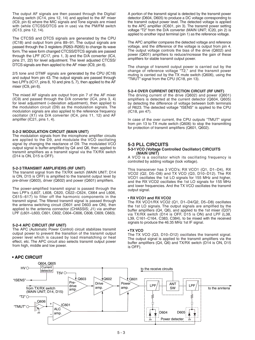
5-2-4 APC CIRCUIT (RF UNIT)
The APC (Automatic Power Control) circuit stabilizes transmit output power to prevent the transition of the transmit output power level which is caused by load mismatching or heat effect, etc. The APC circuit also selects transmit output power from high, middle and low power.
A portion of the transmit signal is detected by the transmit power detector (D604, D605) to produce a DC voltage corresponding to the transmit output power level. The detected voltage is applied to the APC amplifier (IC601, pin 3). The transmit power setting voltage “T2” from the D/A converter (MAIN UNIT; IC20, pin 2) is applied to another input terminal (pin 1) as the reference voltage.
The APC amplifier compares the detected voltage and reference voltage, and the difference of the voltage is output from pin 4. The output voltage controls the bias of the drive (Q602) and power (Q601) amplifiers to reduce/increase the gain of these amplifiers for stable transmit output power.
The change of transmit output power is carried out by the change of reference voltage "T2," and the transmit power muting is carried out by the TX mute switch (Q606), using the “TMUT” signal from the CPU (IC18, pin 13).
In case of the over current, the CPU outputs "TMUT" signal from pin 13 to TX mute switch (Q606) to stop the transmitting for protection of transmit amplifi ers (Q601, Q602).
5-3 PLL CIRCUITS
5-3-1VCO (Voltage Controlled Oscillator) CIRCUITS (MAIN UNIT)
A VCO is a oscillator which its oscillating frequency is controlled by adding voltage (lock voltage).
This transceiver has 3 VCO’s; RX VCO1 (Q1, D1−D4), RX VCO2 (Q2, D5−D8) and TX VCO (Q3, D10−D12). The RX VCO1 oscillates the 1st LO signals for 155 MHz and higher, and the RX VCO2 oscillates the 1st LO signals for 155 MHz and lower frequencies. And the TX VCO oscillates the transmit output signal.
• RX VCO1 and RX VCO2
The RX VCO1/RX VCO2 (Q1, D1−D4/Q2, D5−D8) oscillates the 1st LO signals. The output signals are amplified by the buffer amplifi ers (Q4, Q6), and applied to the 1st mixer (Q37) via TX/RX switch (D14 is OFF, D15 is ON) and LPF (L38, L39, C161−C164, C383, C384), to be mixed with the received signals to produce the 46.35 MHz 1st IF signal.
• TX VCO
The TX VCO (Q3, D10−D12) oscillates the transmit signal. The output signal is applied to the transmit amplifi ers via the buffer amplifi ers (Q4, Q6) and TX/RX switch (D14 is ON, D15 is OFF).
• APC CIRCUIT
| Q604, Q605 |
|
|
|
|
|
|
| |
HV | Current |
|
|
|
| to the receive circuits |
| ||
| detector | T5V |
|
|
|
|
|
| |
|
|
|
|
|
|
|
|
| |
“ISENS” |
|
|
| Q603 | Q602 | Q601 |
|
|
|
|
|
| Pre- | Drive | Power |
| ANT |
| |
|
|
|
| LPF | LPF | ||||
| from TX/RX switch |
| drive | amp. | amp. | SW | |||
|
| amp. |
| to the anntena | |||||
| (MAIN UNIT; D14, D15) |
|
|
|
|
| |||
|
|
|
|
|
|
| |||
“T2” |
|
|
|
|
|
|
|
|
|
| Q606 | + | IC601 |
|
|
|
|
| |
“TMUT” |
|
|
|
|
|
| |||
|
|
|
|
|
|
| |||
| ALC |
|
|
|
|
|
| ||
|
|
|
|
| D604 | D605 |
| ||
|
| – amp. |
|
|
|
| |||
|
|
|
|
|
|
| Power detecter |
| |
5 - 3