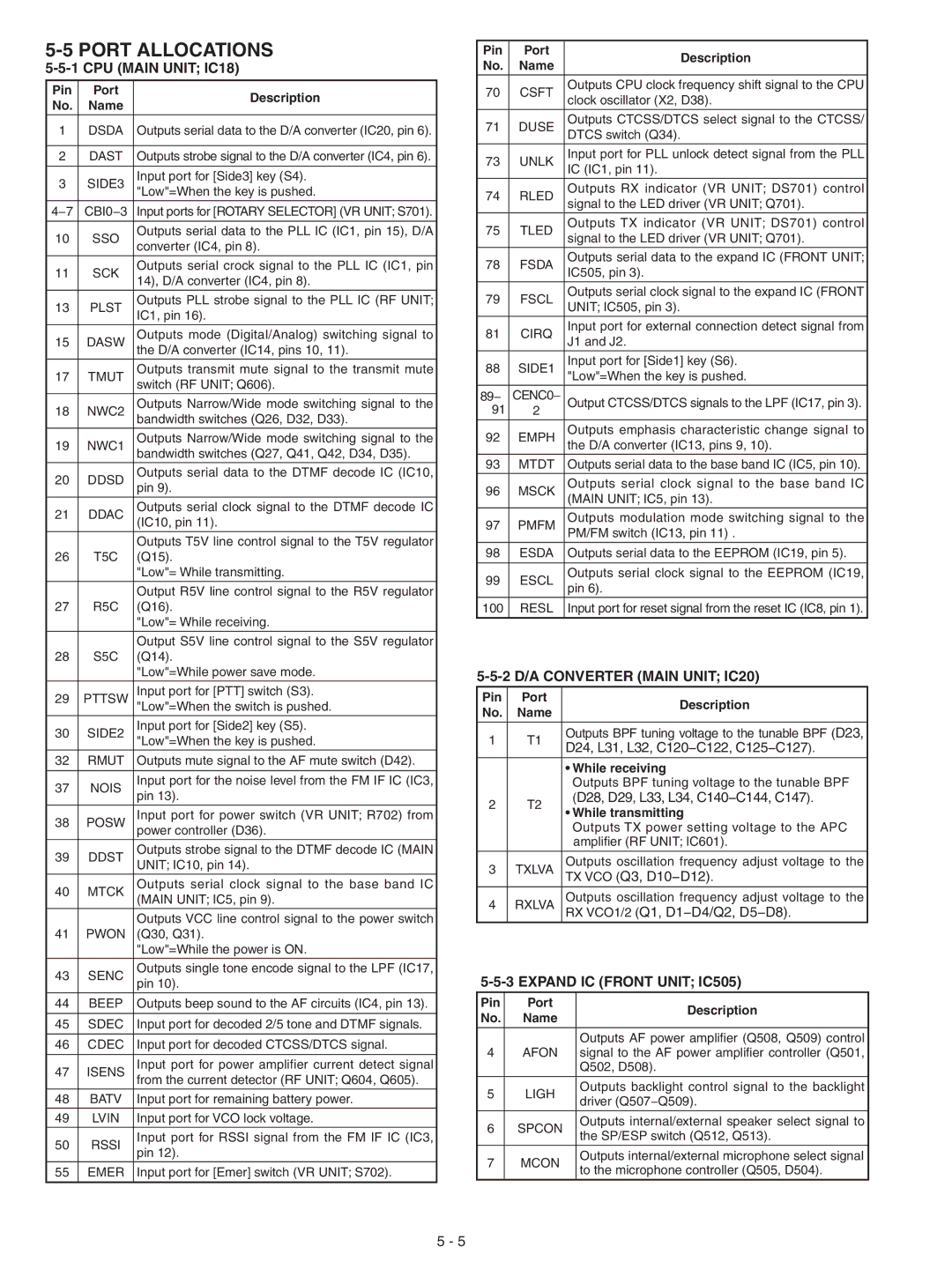
5-5 PORT ALLOCATIONS
5-5-1 CPU (MAIN UNIT; IC18)
Pin | Port | Description | |
No. | Name | ||
| |||
1 | DSDA | Outputs serial data to the D/A converter (IC20, pin 6). | |
|
|
| |
2 | DAST | Outputs strobe signal to the D/A converter (IC4, pin 6). | |
|
|
| |
3 | SIDE3 | Input port for [Side3] key (S4). | |
|
| "Low"=When the key is pushed. | |
4−7 | CBI0−3 | Input ports for [ROTARY SELECTOR] (VR UNIT; S701). | |
|
|
| |
10 | SSO | Outputs serial data to the PLL IC (IC1, pin 15), D/A | |
converter (IC4, pin 8). | |||
|
| ||
|
|
| |
11 | SCK | Outputs serial crock signal to the PLL IC (IC1, pin | |
14), D/A converter (IC4, pin 8). | |||
|
| ||
13 | PLST | Outputs PLL strobe signal to the PLL IC (RF UNIT; | |
IC1, pin 16). | |||
|
| ||
15 | DASW | Outputs mode (Digital/Analog) switching signal to | |
|
| the D/A converter (IC14, pins 10, 11). | |
17 | TMUT | Outputs transmit mute signal to the transmit mute | |
switch (RF UNIT; Q606). | |||
|
| ||
|
|
| |
18 | NWC2 | Outputs Narrow/Wide mode switching signal to the | |
bandwidth switches (Q26, D32, D33). | |||
19 | NWC1 | Outputs Narrow/Wide mode switching signal to the | |
bandwidth switches (Q27, Q41, Q42, D34, D35). | |||
20 | DDSD | Outputs serial data to the DTMF decode IC (IC10, | |
pin 9). | |||
|
|
| |
21 | DDAC | Outputs serial clock signal to the DTMF decode IC | |
(IC10, pin 11). | |||
|
| ||
|
|
| |
|
| Outputs T5V line control signal to the T5V regulator | |
26 | T5C | (Q15). | |
|
| "Low"= While transmitting. | |
|
| Output R5V line control signal to the R5V regulator | |
27 | R5C | (Q16). | |
|
| "Low"= While receiving. | |
|
|
| |
|
| Output S5V line control signal to the S5V regulator | |
28 | S5C | (Q14). | |
|
| "Low"=While power save mode. | |
29 | PTTSW | Input port for [PTT] switch (S3). | |
|
| "Low"=When the switch is pushed. | |
30 | SIDE2 | Input port for [Side2] key (S5). | |
|
| "Low"=When the key is pushed. | |
32 | RMUT | Outputs mute signal to the AF mute switch (D42). | |
|
|
| |
37 | NOIS | Input port for the noise level from the FM IF IC (IC3, | |
pin 13). | |||
|
| ||
|
|
| |
38 | POSW | Input port for power switch (VR UNIT; R702) from | |
power controller (D36). | |||
|
|
| |
39 | DDST | Outputs strobe signal to the DTMF decode IC (MAIN | |
UNIT; IC10, pin 14). | |||
|
| ||
40 | MTCK | Outputs serial clock signal to the base band IC | |
(MAIN UNIT; IC5, pin 9). | |||
|
| Outputs VCC line control signal to the power switch | |
41 | PWON | (Q30, Q31). | |
|
| "Low"=While the power is ON. | |
|
|
| |
43 | SENC | Outputs single tone encode signal to the LPF (IC17, | |
pin 10). | |||
|
| ||
44 | BEEP | Outputs beep sound to the AF circuits (IC4, pin 13). | |
|
|
| |
45 | SDEC | Input port for decoded 2/5 tone and DTMF signals. | |
|
|
| |
46 | CDEC | Input port for decoded CTCSS/DTCS signal. | |
|
|
| |
47 | ISENS | Input port for power amplifier current detect signal | |
from the current detector (RF UNIT; Q604, Q605). | |||
|
|
| |
48 | BATV | Input port for remaining battery power. | |
|
|
| |
49 | LVIN | Input port for VCO lock voltage. | |
50 | RSSI | Input port for RSSI signal from the FM IF IC (IC3, | |
pin 12). | |||
|
| ||
55 | EMER | Input port for [Emer] switch (VR UNIT; S702). | |
|
|
|
Pin | Port | Description | |
No. | Name | ||
| |||
|
|
| |
70 | CSFT | Outputs CPU clock frequency shift signal to the CPU | |
clock oscillator (X2, D38). | |||
|
| ||
|
|
| |
71 | DUSE | Outputs CTCSS/DTCS select signal to the CTCSS/ | |
DTCS switch (Q34). | |||
|
| ||
73 | UNLK | Input port for PLL unlock detect signal from the PLL | |
IC (IC1, pin 11). | |||
|
| ||
74 | RLED | Outputs RX indicator (VR UNIT; DS701) control | |
signal to the LED driver (VR UNIT; Q701). | |||
|
| ||
|
|
| |
75 | TLED | Outputs TX indicator (VR UNIT; DS701) control | |
signal to the LED driver (VR UNIT; Q701). | |||
|
| ||
|
|
| |
78 | FSDA | Outputs serial data to the expand IC (FRONT UNIT; | |
IC505, pin 3). | |||
|
| ||
79 | FSCL | Outputs serial clock signal to the expand IC (FRONT | |
UNIT; IC505, pin 3). | |||
|
| ||
81 | CIRQ | Input port for external connection detect signal from | |
J1 and J2. | |||
|
| ||
|
|
| |
88 | SIDE1 | Input port for [Side1] key (S6). | |
"Low"=When the key is pushed. | |||
|
|
| |
89− | CENC0− | Output CTCSS/DTCS signals to the LPF (IC17, pin 3). | |
91 | 2 |
| |
92 | EMPH | Outputs emphasis characteristic change signal to | |
the D/A converter (IC13, pins 9, 10). | |||
93 | MTDT | Outputs serial data to the base band IC (IC5, pin 10). | |
96 | MSCK | Outputs serial clock signal to the base band IC | |
(MAIN UNIT; IC5, pin 13). | |||
|
|
| |
97 | PMFM | Outputs modulation mode switching signal to the | |
|
| PM/FM switch (IC13, pin 11) . | |
98 | ESDA | Outputs serial data to the EEPROM (IC19, pin 5). | |
|
|
| |
99 | ESCL | Outputs serial clock signal to the EEPROM (IC19, | |
pin 6). | |||
|
| ||
|
|
| |
100 | RESL | Input port for reset signal from the reset IC (IC8, pin 1). |
5-5-2 D/A CONVERTER (MAIN UNIT; IC20)
Pin | Port | Description | |
No. | Name | ||
| |||
|
|
| |
1 | T1 | Outputs BPF tuning voltage to the tunable BPF (D23, | |
D24, L31, L32, C120−C122, C125−C127). | |||
|
| ||
|
| • While receiving | |
|
| Outputs BPF tuning voltage to the tunable BPF | |
2 | T2 | (D28, D29, L33, L34, C140−C144, C147). | |
• While transmitting | |||
|
| ||
|
| Outputs TX power setting voltage to the APC | |
|
| amplifi er (RF UNIT; IC601). | |
3 | TXLVA | Outputs oscillation frequency adjust voltage to the | |
TX VCO (Q3, D10−D12). | |||
|
|
| |
4 | RXLVA | Outputs oscillation frequency adjust voltage to the | |
RX VCO1/2 (Q1, D1−D4/Q2, D5−D8). |
5-5-3 EXPAND IC (FRONT UNIT; IC505)
Pin | Port | Description | |
No. | Name | ||
| |||
|
| Outputs AF power amplifi er (Q508, Q509) control | |
4 | AFON | signal to the AF power amplifi er controller (Q501, | |
|
| Q502, D508). | |
|
|
| |
5 | LIGH | Outputs backlight control signal to the backlight | |
driver (Q507−Q509). | |||
|
| ||
|
|
| |
6 | SPCON | Outputs internal/external speaker select signal to | |
the SP/ESP switch (Q512, Q513). | |||
|
| ||
|
|
| |
7 | MCON | Outputs internal/external microphone select signal | |
to the microphone controller (Q505, D504). | |||
|
|
5 - 5