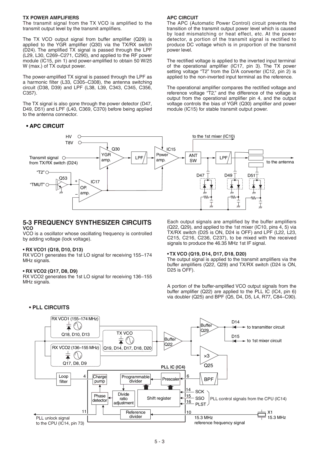
TX POWER AMPLIFIERS
The transmit signal from the TX VCO is amplified to the transmit output level by the transmit amplifi ers.
The TX VCO output signal from buffer amplifier (Q29) is applied to the YGR amplifier (Q30) via the TX/RX switch (D24). The amplified TX signal is passed through the LPF (L29, L30, C269−C271, C290), and applied to the RF power module (IC15, pin 1) and
The
The TX signal is also gone through the power detector (D47, D49, D51) and LPF (L40, C369, C370) before being applied to the antenna connector.
APC CIRCUIT
The APC (Automatic Power Control) circuit prevents the transition of the transmit output power level which is caused by load mismatching or heat effect, etc. At the power detector, a portion of the transmit signal is rectified to produce DC voltage which is in proportion of the transmit power level.
The rectified voltage is applied to the inverted input terminal of the operational amplifier (IC17, pin 3). The TX power setting voltage “T2” from the D/A converter (IC12, pin 2) is applied to the
The operational amplifier compares the rectified voltage and reference voltage “T2,” and the difference of the voltage is output from the operational amplifier pin 4, and the output voltage controls the bias of YGR (Q30) amplifier and power module (IC15) for stable transmit output power.
• APC CIRCUIT
HV |
|
|
|
| to the 1st mixer (IC10) |
| |
T8V |
|
|
|
|
|
|
|
|
| Q30 |
| IC15 |
|
|
|
Transmit signal |
| YGR | LPF | Power | ANT | LPF |
|
| amp. | amp. | SW |
| |||
from TX/RX switch (D24) |
|
|
| ||||
|
|
|
|
|
| ||
“T2” |
|
|
|
| D47 | D49 | D51 |
Q53 |
|
|
|
| |||
+ | IC17 |
|
|
|
|
| |
“TMUT” |
|
|
|
|
| ||
| OP. |
|
|
|
|
| |
|
|
|
|
|
|
| |
| – | amp. |
|
|
|
|
|
to the antenna
5-3 FREQUENCY SYNTHESIZER CIRCUITS
VCO
VCO is a oscillator whose oscillating frequency is controlled by adding voltage (lock voltage).
• RX VCO1 (Q18, D10, D13)
RX VCO1 generates the 1st LO signal for receiving 155−174 MHz signals.
• RX VCO2 (Q17, D8, D9)
RX VCO2 generates the 1st LO signal for receiving 136−155 MHz signals.
Each output signals are amplified by the buffer amplifiers (Q22, Q29), and applied to the 1st mixer (IC10, pins 4, 5) via TX/RX switch (D25 is ON, D24 is OFF) and LPF (L22, L23, C215, C216, C236, C237), to be mixed with the received signals to produce the 46.35 MHz 1st IF signal.
• TX VCO (Q19, D14, D17, D18, D20)
The output signal is applied to the transmit amplifi ers via the buffer amplifi ers (Q22, Q29) and TX/RX switch (D24 is ON, D25 is OFF).
A portion of the
• PLL CIRCUITS
RX VCO1
Q18, D10, D13
RX VCO2
TX VCO
Q19, D14, D17, D18, D20
Buffer
Q22
Buffer | D14 | |
to transmitter circuit | ||
Q29 | ||
| ||
| D15 | |
| to 1st mixer circuit |
×3
| Q17, D8, D9 |
|
|
|
|
|
|
|
|
|
|
|
|
|
|
| PLL IC (IC4) |
|
| Q25 |
|
| ||||||||||
|
|
|
|
|
|
|
|
|
|
|
|
|
|
|
|
|
|
|
|
|
| |||||||||||
|
| 4 |
|
|
|
|
|
|
|
|
|
|
|
|
|
|
|
|
|
|
|
| 6 |
|
|
|
|
|
|
|
|
|
|
|
|
|
|
|
|
|
|
|
|
|
|
|
|
|
|
|
|
|
|
|
|
|
|
|
|
|
|
|
| ||
| Loop |
|
| Charge |
|
|
| Programmable |
|
| Prescaler |
|
|
|
| BPF |
|
|
|
|
|
|
| |||||||||
| filter |
|
|
| pump |
|
|
|
| divider |
|
|
|
|
|
|
|
|
|
|
|
|
|
|
| |||||||
|
|
|
|
|
|
|
|
|
|
|
|
|
|
|
|
|
|
|
|
|
|
|
|
| ||||||||
|
|
|
|
|
|
|
|
|
|
|
|
|
|
|
|
|
|
|
|
|
|
| 14 | SCK |
|
| ||||||
|
|
|
|
| Phase |
| Divide |
|
| Shift register |
|
|
| 15 | SSO PLL control signals from the CPU (IC14) | |||||||||||||||||
|
|
|
|
|
| ratio |
|
|
|
|
| |||||||||||||||||||||
|
|
|
| detector |
|
|
|
|
|
| 16 | |||||||||||||||||||||
|
|
|
|
| adjustment |
|
|
|
|
|
|
|
|
| PLST |
|
| |||||||||||||||
|
|
|
|
|
|
|
|
|
|
|
|
|
|
|
|
|
|
|
|
|
| |||||||||||
|
| 11 |
|
|
|
|
|
|
|
|
|
|
|
|
|
|
|
|
|
|
|
| ||||||||||
|
|
|
|
|
|
|
|
|
|
|
|
|
|
|
|
|
|
|
|
|
|
|
|
|
|
|
|
|
|
|
| |
|
|
|
|
|
|
|
|
|
|
|
| Reference |
|
|
|
|
|
|
| 10 |
|
|
|
|
|
|
|
| X1 | |||
|
|
|
|
|
|
|
|
|
|
|
|
|
|
|
|
|
|
|
|
|
|
|
| |||||||||
PLL unlock signal |
|
|
|
|
|
|
|
|
|
|
| divider |
|
|
|
|
|
|
|
| 15.3 MHz |
|
|
|
| 15.3 MHz | ||||||
to the CPU (IC14, pin 73) |
|
|
|
|
|
|
|
|
|
|
|
|
|
|
|
|
|
|
|
|
| reference frequency signal |
|
| ||||||||
|
|
|
|
|
|
|
|
|
|
|
|
|
|
|
|
|
|
|
|
|
|
| ||||||||||
5 - 3