AP440FX specifications
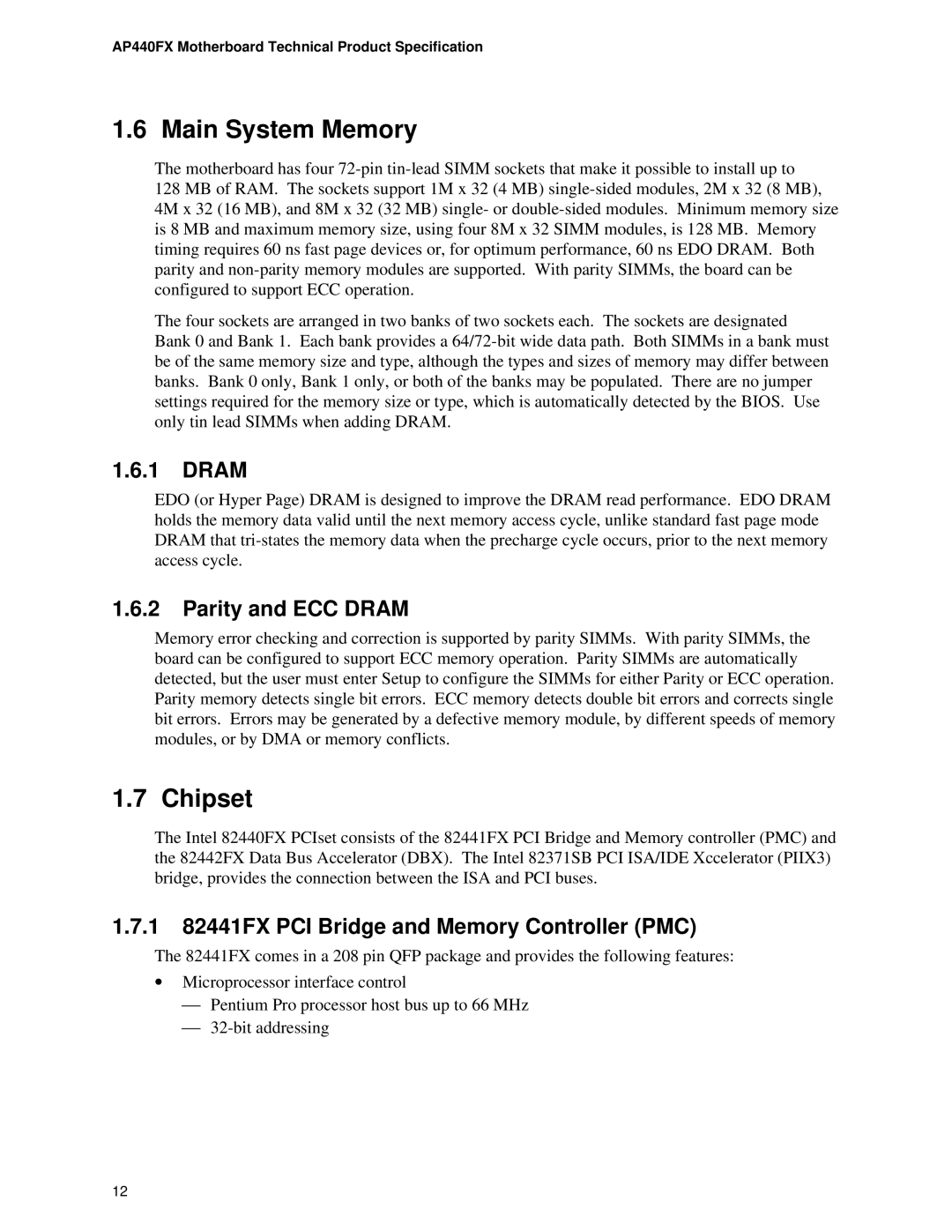
The Intel AP440FX is a pivotal motherboard that was released in the late 1990s, designed to support the Intel Pentium II and Pentium III processors. Known for its robust performance and versatile functionalities, the AP440FX became a popular choice among computer enthusiasts and system builders during its time.One of the defining features of the Intel AP440FX is its support for the Intel 440FX chipset. This chipset provided improved system performance through its use of a 66 MHz front-side bus, which allowed for faster data transfer between the CPU and the memory. The motherboard was equipped with two DIMM slots capable of supporting a maximum of 512 MB of SDRAM, providing users with the flexibility to choose the amount of memory they required for their applications.
Another notable characteristic of the AP440FX motherboard is its integrated support for various peripheral interfaces. It comes equipped with multiple ISA and PCI slots, allowing users to expand their system capabilities through the addition of various cards. The presence of two USB ports, which were relatively new at the time of its release, gave users access to a wider range of peripherals and external devices.
The Intel AP440FX also features an integrated IDE controller, enabling connection for hard drives and optical drives without the need for additional controller cards. This integrated solution simplified storage management for users and contributed to the overall efficiency of the system. The motherboard also supported SCSI through optional daughter cards, catering to users who required high-speed data transfer and reliable disk storage solutions.
Moreover, the AP440FX was designed with future upgrades in mind. Its BIOS supported plug-and-play installations, allowing users to easily configure new hardware components without extensive troubleshooting. Additionally, the ATX form factor of the motherboard contributed to its compatibility with a wide range of cases and power supplies.
In terms of power management, the Intel AP440FX incorporated advanced features such as ACPI (Advanced Configuration and Power Interface), which allowed for better power efficiency and management of power states. This feature was particularly beneficial for users looking to reduce energy consumption and improve the overall longevity of their systems.
All in all, the Intel AP440FX represented a significant advancement in motherboard technology during its era. Its combination of robust performance, upgradeability, and support for new technologies made it a popular choice for users looking to build powerful and efficient computing systems.
