Introducing the |
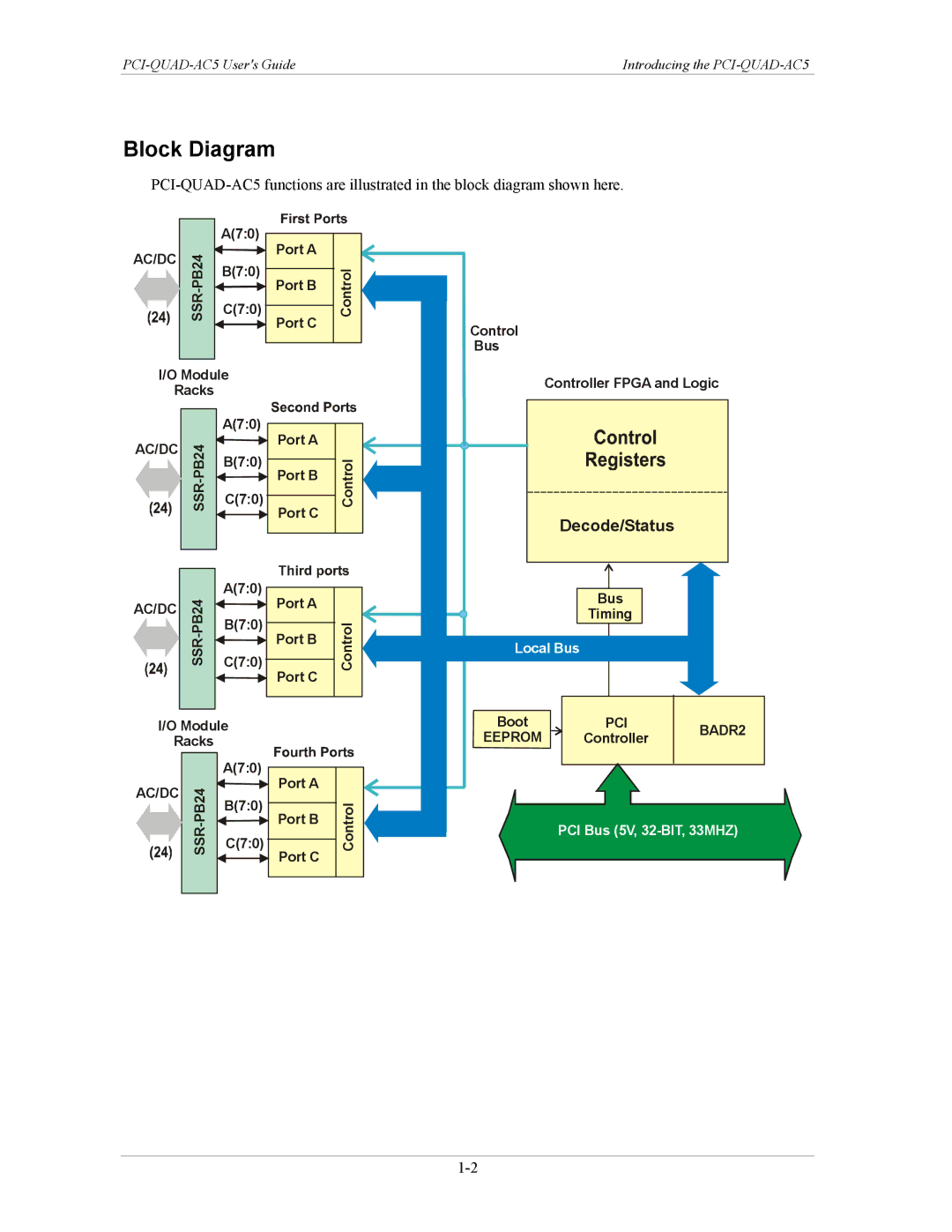
Block Diagram
|
|
| A(7:0) |
|
| ||
AC/DC | Port A |
| |||||
|
|
|
| ||||
|
|
|
|
| |||
|
| C(7:0) |
| Control | |||
|
|
| B(7:0) | Port B |
| ||
|
|
|
|
|
|
| |
|
|
|
|
|
|
|
|
|
|
|
|
|
|
|
|
|
|
|
|
|
| Port C |
|
Control
Bus
I/O Module
Racks
|
|
|
| A(7:0) | ||
AC/DC | PB24 | B(7:0) | ||||
|
|
| ||||
|
|
| SSR- |
| C(7:0) | |
|
|
|
| |||
|
|
|
|
| ||
|
|
|
|
|
|
|
|
|
|
|
|
|
|
|
|
| PB24 | A(7:0) |
AC/DC | B(7:0) | |||
|
| |||
|
|
| SSR- | C(7:0) |
|
|
| ||
|
|
| ||
|
|
|
| |
|
|
|
|
|
Port A | Control | |
Port B | ||
| ||
Port C |
| |
|
|
Port A | Control | |
Port B | ||
| ||
Port C |
| |
|
|
Controller FPGA and Logic
Decode/Status |
Bus |
Timing |
Local Bus |
I/O Module
Racks
|
|
|
| A(7:0) | ||
AC/DC | PB24 | B(7:0) | ||||
|
|
| ||||
|
|
| SSR- |
| C(7:0) | |
|
|
|
| |||
|
|
|
|
| ||
|
|
|
|
|
|
|
|
|
|
|
|
|
|
Port A
Port B
Port C
Control
Boot | PCI | BADR2 | |
EEPROM | Controller | ||
| |||
|
|
|
PCI Bus (5V,