NXP Semiconductors | UM10301 |
| User Manual PCF85x3, PCA8565 and PCF2123, PCA2125 |
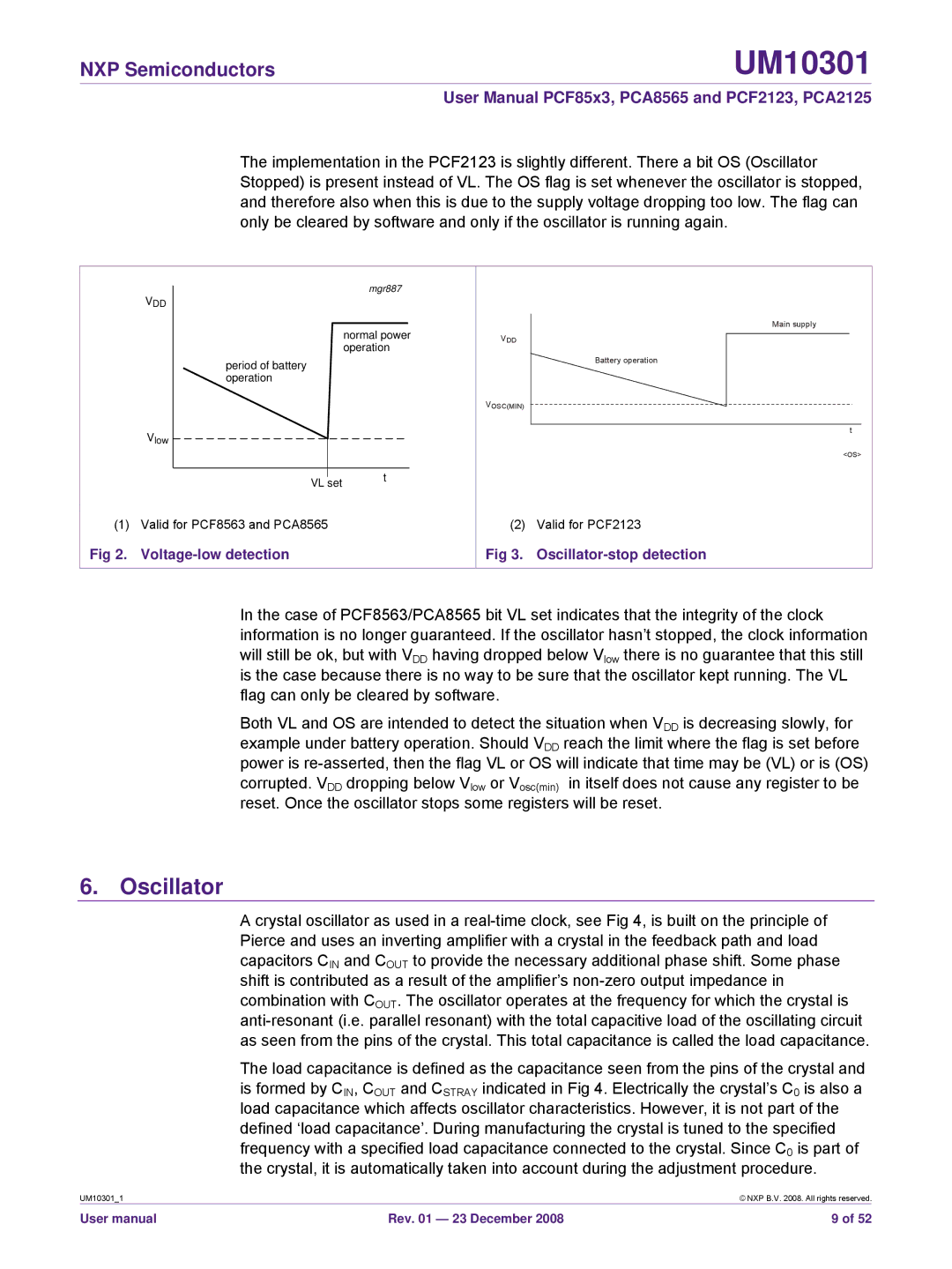
The implementation in the PCF2123 is slightly different. There a bit OS (Oscillator Stopped) is present instead of VL. The OS flag is set whenever the oscillator is stopped, and therefore also when this is due to the supply voltage dropping too low. The flag can only be cleared by software and only if the oscillator is running again.
| mgr887 |
VDD |
|
| normal power |
| operation |
period of battery |
|
operation |
|
Vlow |
|
VL set | t |
|
VDD
VOSC(MIN)
Main supply |
Battery operation |
t |
<OS> |
(1) Valid for PCF8563 and PCA8565
Fig 2. Voltage-low detection
(2) Valid for PCF2123
Fig 3. Oscillator-stop detection
In the case of PCF8563/PCA8565 bit VL set indicates that the integrity of the clock information is no longer guaranteed. If the oscillator hasn’t stopped, the clock information will still be ok, but with VDD having dropped below Vlow there is no guarantee that this still is the case because there is no way to be sure that the oscillator kept running. The VL flag can only be cleared by software.
Both VL and OS are intended to detect the situation when VDD is decreasing slowly, for example under battery operation. Should VDD reach the limit where the flag is set before power is
corrupted. VDD dropping below Vlow or Vosc(min) in itself does not cause any register to be reset. Once the oscillator stops some registers will be reset.
6. Oscillator
A crystal oscillator as used in a
The load capacitance is defined as the capacitance seen from the pins of the crystal and
is formed by CIN, COUT and CSTRAY indicated in Fig 4. Electrically the crystal’s C0 is also a load capacitance which affects oscillator characteristics. However, it is not part of the
defined ‘load capacitance’. During manufacturing the crystal is tuned to the specified frequency with a specified load capacitance connected to the crystal. Since C0 is part of the crystal, it is automatically taken into account during the adjustment procedure.
UM10301_1 |
| © NXP B.V. 2008. All rights reserved. |
User manual | Rev. 01 — 23 December 2008 | 9 of 52 |