1234
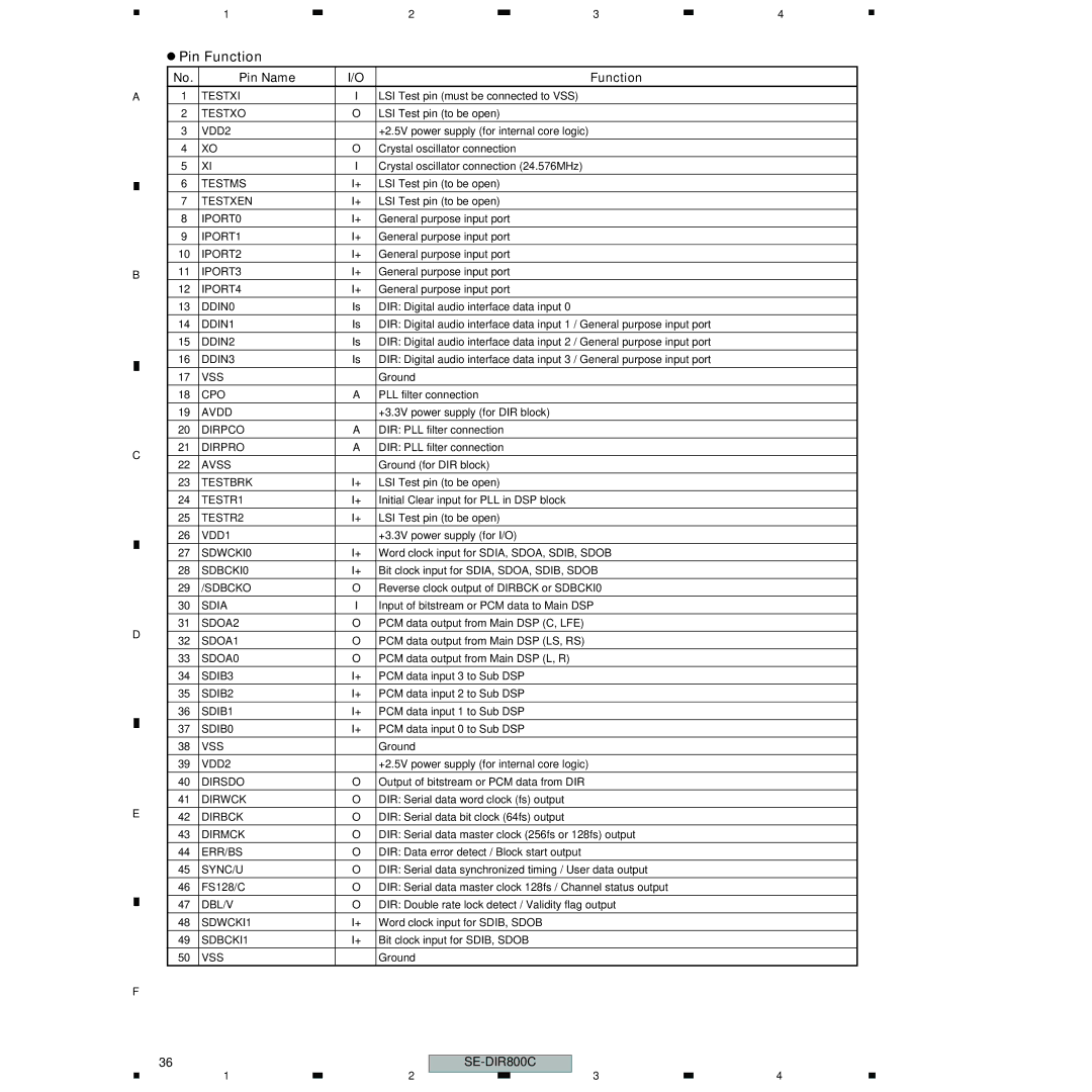
 Pin Function
| No. | Pin Name | I/O | Function | |
A | 1 | TESTXI | I | LSI Test pin (must be connected to VSS) | |
| 2 | TESTXO | O | LSI Test pin (to be open) | |
|
|
|
|
| |
| 3 | VDD2 | − | +2.5V power supply (for internal core logic) | |
|
|
|
|
| |
| 4 | XO | O | Crystal oscillator connection | |
|
|
|
|
| |
| 5 | XI | I | Crystal oscillator connection (24.576MHz) | |
| 6 | TESTMS | I+ | LSI Test pin (to be open) | |
|
|
|
|
| |
| 7 | TESTXEN | I+ | LSI Test pin (to be open) | |
| 8 | IPORT0 | I+ | General purpose input port | |
|
|
|
|
| |
| 9 | IPORT1 | I+ | General purpose input port | |
|
|
|
|
| |
| 10 | IPORT2 | I+ | General purpose input port | |
|
|
|
|
| |
B | 11 | IPORT3 | I+ | General purpose input port | |
|
|
|
| ||
| 12 | IPORT4 | I+ | General purpose input port | |
|
|
|
|
| |
| 13 | DDIN0 | Is | DIR: Digital audio interface data input 0 | |
|
|
|
|
| |
| 14 | DDIN1 | Is | DIR: Digital audio interface data input 1 / General purpose input port | |
|
|
|
|
| |
| 15 | DDIN2 | Is | DIR: Digital audio interface data input 2 / General purpose input port | |
|
|
|
|
| |
| 16 | DDIN3 | Is | DIR: Digital audio interface data input 3 / General purpose input port | |
| 17 | VSS | − | Ground | |
|
|
|
|
| |
| 18 | CPO | A | PLL filter connection | |
|
|
|
|
| |
| 19 | AVDD | − | +3.3V power supply (for DIR block) | |
| 20 | DIRPCO | A | DIR: PLL filter connection | |
C | 21 | DIRPRO | A | DIR: PLL filter connection | |
22 | AVSS | − | Ground (for DIR block) | ||
| |||||
| 23 | TESTBRK | I+ | LSI Test pin (to be open) | |
|
|
|
|
| |
| 24 | TESTR1 | I+ | Initial Clear input for PLL in DSP block | |
|
|
|
|
| |
| 25 | TESTR2 | I+ | LSI Test pin (to be open) | |
|
|
|
|
| |
| 26 | VDD1 | − | +3.3V power supply (for I/O) | |
|
|
|
|
| |
| 27 | SDWCKI0 | I+ | Word clock input for SDIA, SDOA, SDIB, SDOB | |
|
|
|
|
| |
| 28 | SDBCKI0 | I+ | Bit clock input for SDIA, SDOA, SDIB, SDOB | |
|
|
|
|
| |
| 29 | /SDBCKO | O | Reverse clock output of DIRBCK or SDBCKI0 | |
| 30 | SDIA | I | Input of bitstream or PCM data to Main DSP | |
D | 31 | SDOA2 | O | PCM data output from Main DSP (C, LFE) | |
32 | SDOA1 | O | PCM data output from Main DSP (LS, RS) | ||
| |||||
|
|
|
|
| |
| 33 | SDOA0 | O | PCM data output from Main DSP (L, R) | |
|
|
|
|
| |
| 34 | SDIB3 | I+ | PCM data input 3 to Sub DSP | |
|
|
|
|
| |
| 35 | SDIB2 | I+ | PCM data input 2 to Sub DSP | |
| 36 | SDIB1 | I+ | PCM data input 1 to Sub DSP | |
| 37 | SDIB0 | I+ | PCM data input 0 to Sub DSP | |
| 38 | VSS | − | Ground | |
| 39 | VDD2 | − | +2.5V power supply (for internal core logic) | |
| 40 | DIRSDO | O | Output of bitstream or PCM data from DIR | |
| 41 | DIRWCK | O | DIR: Serial data word clock (fs) output | |
E | 42 | DIRBCK | O | DIR: Serial data bit clock (64fs) output | |
| 43 | DIRMCK | O | DIR: Serial data master clock (256fs or 128fs) output | |
| 44 | ERR/BS | O | DIR: Data error detect / Block start output | |
| 45 | SYNC/U | O | DIR: Serial data synchronized timing / User data output | |
| 46 | FS128/C | O | DIR: Serial data master clock 128fs / Channel status output | |
| 47 | DBL/V | O | DIR: Double rate lock detect / Validity flag output | |
| 48 | SDWCKI1 | I+ | Word clock input for SDIB, SDOB | |
| 49 | SDBCKI1 | I+ | Bit clock input for SDIB, SDOB | |
| 50 | VSS | − | Ground |
F
36
1 | 2 |
3 | 4 |
