General Information |
|
|
|
|
|
|
|
| DDR3 SDRAM | ||
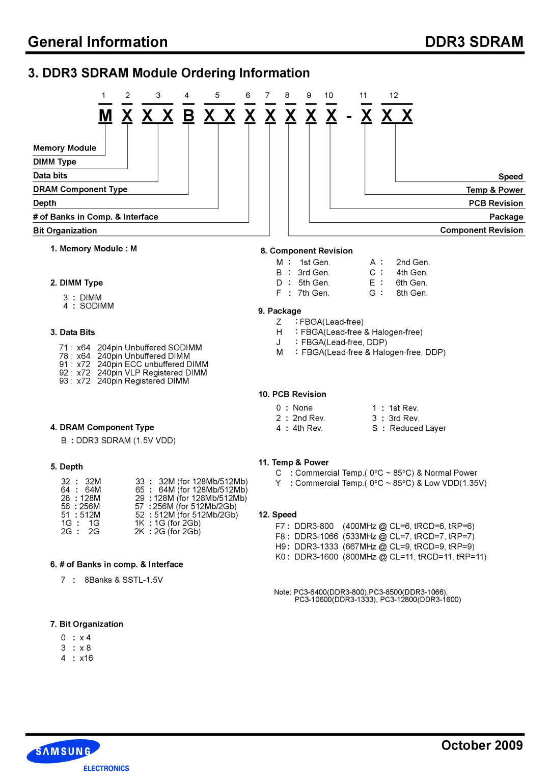
3. DDR3 SDRAM Module Ordering Information |
|
|
| ||||||||
1 | 2 | 3 | 4 | 5 | 6 | 7 | 8 | 9 | 10 | 11 | 12 |
M X X X B X X X X X X X - X X X
Memory Module
DIMM Type
Data bits
DRAM Component Type
Depth
#of Banks in Comp. & Interface Bit Organization
1.Memory Module : M
2.DIMM Type
3 : DIMM
4 : SODIMM
3.Data Bits
71 : x64 204pin Unbuffered SODIMM
78 : x64 240pin Unbuffered DIMM
91 : x72 240pin ECC unbuffered DIMM
92 : x72 240pin VLP Registered DIMM
93 : x72 240pin Registered DIMM
4.DRAM Component Type
B : DDR3 SDRAM (1.5V VDD)
Speed
Temp & Power
PCB Revision
Package
Component Revision
8. Component Revision |
|
|
| ||
M | : | 1st Gen. | A : | 2nd Gen. | |
B | : | 3rd Gen. | C | : | 4th Gen. |
D | : | 5th Gen. | E | : | 6th Gen. |
F | : | 7th Gen. | G : | 8th Gen. | |
9. Package
Z | : |
H | : |
J | : |
M:
10.PCB Revision
0 | : | None | 1 | : | 1st Rev. |
2 | : | 2nd Rev. | 3 | : | 3rd Rev. |
4 | : | 4th Rev. | S : | Reduced Layer | |
5. Depth |
|
|
|
| 11. Temp & Power |
| ||||
|
|
|
| C : Commercial Temp.( 0°C ~ 85°C) & Normal Power | ||||||
32 | : | 32M | 33 | : | 32M (for 128Mb/512Mb) | |||||
Y |
| ° | ° | |||||||
64 | : | 64M | 65 | : | 64M (for 128Mb/512Mb) |
| : Commercial Temp.( 0 C ~ 85 C) & Low VDD(1.35V) | |||
28 | : 128M | 29 | : 128M (for 128Mb/512Mb) |
|
|
|
| |||
56 | : 256M | 57 : 256M (for 512Mb/2Gb) | 12. Speed |
| ||||||
51 | : 512M | 52 | : 512M (for 512Mb/2Gb) |
| ||||||
1G : | 1G | 1K | : 1G (for 2Gb) | F7 | : | |||||
2G : | 2G | 2K | : 2G (for 2Gb) | |||||||
F8 | : | |||||||||
|
|
|
|
|
| |||||
|
|
|
|
|
| H9 : | ||||
6. # of Banks in comp. & Interface | K0 : | |||||||||
|
|
|
| |||||||
7 | : | 8Banks & |
|
|
|
| ||||
|
|
|
|
|
| Note: | ||||
|
|
|
|
|
|
|
| |||
7. Bit Organization
0: x 4
3: x 8
4: x16
October 2009