2 HARDWARE IMPLEMENTATION | |
|
|
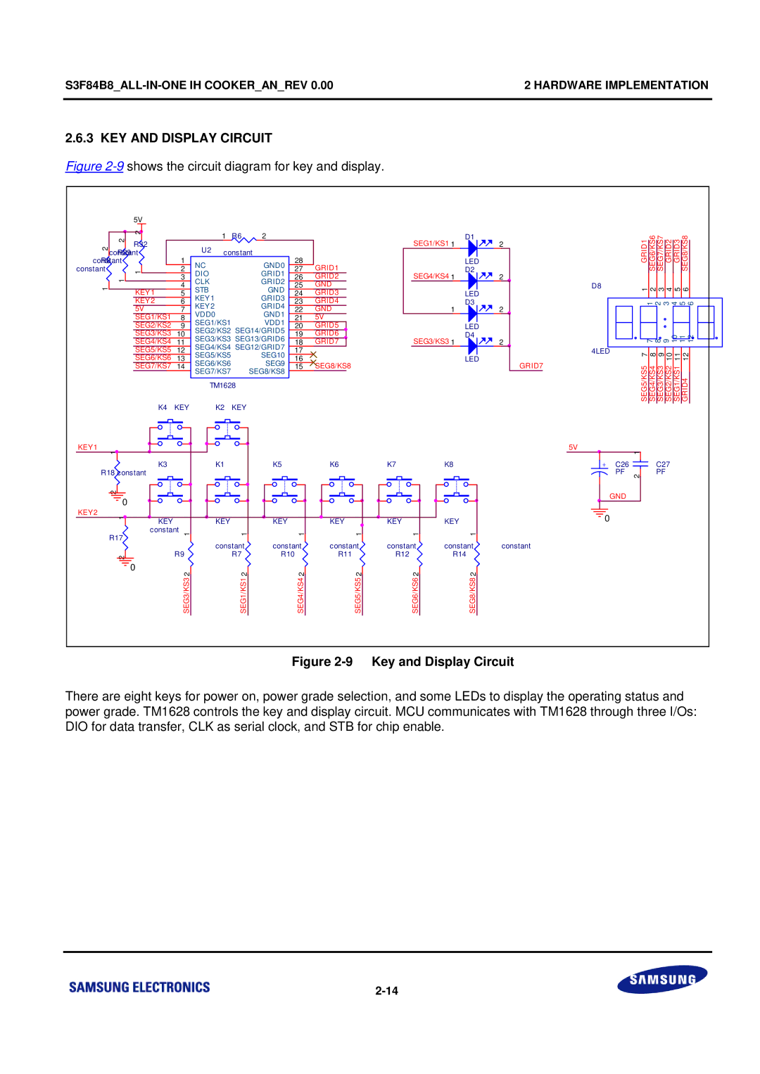
2.6.3 KEY AND DISPLAY CIRCUIT
Figure 2-9 shows the circuit diagram for key and display.
|
|
| 5V |
|
|
|
|
|
|
|
|
|
|
|
|
|
|
| |||
|
|
|
|
|
|
|
|
|
|
|
|
|
|
|
|
|
|
|
|
|
|
| 2 | 2 |
|
|
|
|
|
| 1 | R6 | 2 |
|
|
|
| ||||||
|
|
|
|
|
|
|
|
|
|
|
|
| |||||||||
|
|
|
|
|
|
|
|
|
|
|
|
|
|
|
|
|
|
|
|
| |
2 |
|
| R32 |
|
|
|
| U2 constant |
|
|
|
| |||||||||
| constantR29 |
| 1 | 28 |
|
|
| ||||||||||||||
constantR8 |
|
|
|
|
| NC |
|
|
| GND0 |
| GRID1 |
| ||||||||
constant |
| 1 |
|
|
| 2 | DIO |
|
|
| GRID1 | 27 |
| ||||||||
| 1 |
|
|
|
|
| 3 | CLK |
|
|
| GRID2 | 26 |
| GRID2 |
| |||||
1 |
|
|
|
|
|
| 4 | STB |
|
|
|
| GND | 25 |
| GND |
| ||||
|
|
| KEY1 |
| 5 |
|
|
|
| 24 |
| GRID3 |
| ||||||||
|
|
| KEY 1 |
|
|
| GRID3 |
| |||||||||||||
|
|
| KEY2 |
| 6 |
|
|
| 23 |
| GRID4 |
| |||||||||
|
|
| KEY 2 |
|
|
| GRID4 |
| |||||||||||||
|
|
| 5V | 7 |
|
|
| 22 |
| GND | |||||||||||
|
|
| VDD0 |
|
|
| GND1 |
| |||||||||||||
|
|
| SEG1/KS1 |
| 8 |
|
|
| 21 |
| 5V |
| |||||||||
|
|
| SEG2/KS2 | 9 | SEG1/KS1 |
|
|
|
| VDD1 | 20 |
| GRID5 |
| |||||||
|
|
| SEG2/KS2 SEG14/GRID5 |
|
| ||||||||||||||||
|
|
|
|
|
|
|
|
|
|
|
|
|
| ||||||||
|
|
| SEG3/KS3 | 10 | 19 |
| GRID6 |
| |||||||||||||
|
|
| SEG3/KS3 SEG13/GRID6 |
|
| ||||||||||||||||
|
|
|
|
|
|
|
|
|
|
|
|
|
| ||||||||
|
|
| SEG4/KS4 | 11 | 18 |
| GRID7 |
| |||||||||||||
|
|
| SEG4/KS4 SEG12/GRID7 |
|
| ||||||||||||||||
|
|
|
|
|
|
|
|
|
|
|
|
|
| ||||||||
|
|
| SEG5/KS5 | 12 | 17 |
|
|
| |||||||||||||
|
|
| SEG5/KS5 |
|
|
| SEG10 |
|
|
| |||||||||||
|
|
|
|
|
|
|
|
|
|
|
|
|
|
|
|
| |||||
|
|
| SEG6/KS6 | 13 |
|
|
| 16 |
|
|
| ||||||||||
|
|
| SEG6/KS6 |
|
|
|
| SEG9 |
|
|
| ||||||||||
|
|
|
|
|
|
|
|
|
|
|
|
|
|
|
|
|
| ||||
|
|
| SEG7/KS7 | 14 |
|
|
|
| 15 |
| SEG8/KS8 | ||||||||||
|
|
| SEG7/KS7 |
|
| SEG8/KS8 |
| ||||||||||||||
|
|
|
|
|
|
|
|
|
|
|
|
|
|
|
| ||||||
|
|
|
|
|
|
|
|
|
| TM1628 |
|
|
|
|
|
|
| ||||
|
|
|
|
| K4 |
| KEY |
| K2 | KEY |
|
|
|
|
|
|
| ||||
|
|
|
|
|
|
|
|
|
|
|
|
|
|
|
|
|
|
|
|
|
|
|
|
|
|
|
|
|
|
|
|
|
|
|
|
|
|
|
|
|
|
|
|
SEG1/KS1 1 | D1 |
2 | |
| LED |
SEG4/KS4 1 | D2 |
2 | |
| LED |
1 | D3 |
2 | |
| LED |
SEG3/KS3 1 | D4 |
2 |
LED
D8
4LED
GRID7
SEG5/KS5 71 GRID1 SEG4/KS4 8 7 1 2 SEG6/KS6 SEG3/KS3 9 8 2 3 SEG7/KS7 SEG2/KS2 10 9 3 4 GRID2 SEG1/KS1 11 10 4 5 GRID3 GRID4 12 11 5 6 SEG8/KS8 12 6
KEY1
KEY2
1![]()
R18 constant
2
0
1![]()
R17![]()
2
0
K3
![]() KEY constant 1
KEY constant 1
R9 ![]()
SEG3/KS3 2
K1 | K5 | K6 | K7 |
KEY | KEY | KEY | KEY |
1 | 1 | 1 | 1 |
constant | constant | constant | constant |
R7 | R10 | R11 | R12 |
2 | 2 | 2 | 2 |
SEG1/KS1 | SEG4/KS4 | SEG5/KS5 | SEG6/KS6 |
| 5V |
|
K8 | + | C26 |
|
| PF |
|
| GND |
KEY | 0 | |
1 |
|
|
constant | constant |
|
R14 |
|
|
2 |
|
|
SEG8/KS8 |
|
|
2 1![]()
C27
PF
Figure 2-9 Key and Display Circuit
There are eight keys for power on, power grade selection, and some LEDs to display the operating status and power grade. TM1628 controls the key and display circuit. MCU communicates with TM1628 through three I/Os: DIO for data transfer, CLK as serial clock, and STB for chip enable.