928-998-12
Specifications
SELF-DIAGNOSIS Function
Items of Error History Mode Items and Contents
AEP, UK
Flexible Circuit Board Repairing
HK, SP, MY, AR, AUS, KR, JE
Disassembly
Table of Contents
Diagrams
Exploded Views
Cleaning the Optical Pickup CD Player
Drawing OUT the Tray During Power OFF
Section Servicing Note
Removing the Indication Plate FL
Service Position the Power Board
Hot Reset
Cold Reset
LED and Fluorescent Indicator Tube All Lit, Key Check Mode
Change-over of AM tuner Step between 9kHz and 10kHz
Error History Display Mode
Aging Mode
Reading the BD Error History Display
Reading the Mechanism Error History Display
IOP
JIG for Checking BD MD Board Waveform
TEO
Record Precedure
Forced Reset
Checks Prior to Parts Replacement and Adjustments
REC/PLAY
Main Board Component Side
Tuning +/MD/CD/TUNING +
Retry Cause Display Mode
Hexadecimal nBinary Conversion Table
Location of Parts and Controls
Section General
Front Panel
Page
Page
Case
Section Disassembly
Back Panel
Front Panel
CD Mechanism Deck
Main Board and Power Transformer
CD Base Unit
TRAY, Gear and CAM
Optical PICK-UP Section of CD KSS-213BA/F-NP
MD Mechanism Deck
BD CD BOARD, Spindle Motor M101 and Sled Motor M102
Set the shaft of Cam gear to
Spindle Motor M901 and Sled Motor M902 MD
Over Write Head Optical PICK-UP of MD KMS-260B/J1N
Precautions for USE of Test Mode
Section Test Mode
Setting the Test Mode
Exiting the Test Mode
Display Contents Mark Group
Selecting the Test Mode
Non-Volatile Memory Mode EEP Mode
Operating the Continuous Playback Mode
MID
OUT
Functions of Other Buttons
Test Mode Displays
Meanings of Other Displays
MD Section Parts Replacement and Adjustment
Section Electrical Adjustments
Precautions for USE of Optical PICK- UP KMS-260B
Precautions for Checking Laser Diode Emissinon
Precautions for Adjustments
Creating Continuously Recorded Disc
Laser Power Check
Temperature Compensation Offset Check
Checks Prior to Repairs
Specified Value
CD Error Rate Check
Play Checking MO Error Rate Check
Focus Bias Check
Self-Recording/playback Check
Temperature Compensation Offset Adjutment
Initial Setting of Adjustment Value
Laser Power Adjustment
Recording and Displaying the IOP Information
Check
Traverse Adjustment
Press the ENTER/YES R button, display EFB =
Focus Bias Adjustment
Auto Gain Control Output Level Adjustment
Error Rate Check
CD Auto Gain Control Output Level Adjustment
MO Auto Gain Control Output Level Adjustment
CD Section
Adjusting Points and Connecting Points
Curve Check
RF Level Check
Circuit Boards Location
HCD-MD373 Section Diagrams
HCD-MD373
Block Diagrams BD CD Section
REC
BD MD /2
D/A Converter
BD CD Section
Main Section
BD MD 1/2 Section
Waveforms BD CD Section
BD MD 2/2 Section
Main 3/3 Section
See page 40 for Circuit Boards Location
Printed Wiring Board BD CD Section
Main Board
Schematic Diagram BD CD Section
Semiconductor Location
Printed Wiring Board BD MD Section
Schematic Diagram BD MD /2
MD Digital Board
Schematic Diagram SP Section Printed Wiring Board SP Section
Printed Wiring Board Main Section
See page 68 for IC Block Diagrams
Schematic Diagram Main /3
HCD-MD373
HCD-MD373
See page 45 for Waveforms See page 67 for IC Block Diagrams
Schematic Diagram MD Digital Section
Printed Wiring Board MD Digital Section
Schematic Diagram AMP Section
Printed Wiring Board AMP Section
Schematic Diagram Panel Section
Printed Wiring Board Panel Section
Schematic Diagram Power Section
AEP, UK
Printed Wiring Board Power Section
Except AEP, UK Voltage Selector
Printed Wiring Board BD Switch Section
Schematic Diagram BD Switch Section
Schematic Diagram Loading Section
Printed Wiring Board Loading Section
BD MD Board 1/2 IC101 CXA2523AR
IC Block Diagrams
BD MD Board 2/2 IC121 CXD2654R
IC152 BH6511FS-E2
C103 CXA2568M-T6 MD Digital Board
BD CD Board IC101 CXD2587Q
IC153 LB1830M-S-TE-L
Main Board 1/3 IC302 MC14052B
Main Board 3/3 IC171 LB1641
Main Board 2/3 IC301 M62428AFP IC931 M62016L
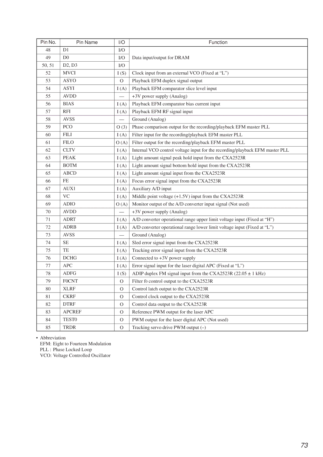
IC PIN Functions
IC101 Digital Signal Processor CXD2587Q Bdcd board
Adio
Rfdc
AVSS0
Igen
IC101 RF Amplifier CXA2523AR Bdmd board
MNT1 Shck
MNT0 FOK
MNT2 Xbusy
MNT3 Sloc
Avdd
Mvci
RFI
Avss
Sprd
FS4
Spfd
Fgin
IC501 Master Control M30620ECFP-A21 Main board
Stereo
CD-RESET
Tuned
ST-CE
Case and Front Panel Section
Section Exploded Views
59 #3
Chassis Section
113 110 107
MD Mechanism Deck MDM-5A
125 126 106 105
MD Base Unit MBU-5A
CD Mechanism Deck CDM55A-5SBD32
255 256 257 253 254
CD Base Unit BU-5SBD32
252 254
258 251
CD Mechanism Deck CDM55C-5BD32
355 356 357 353 354
CD Base Unit BU-5BD32
352 354
358 351
Section Electrical Parts List AMP
AMP BD CD
BD CD BD MD
Inductor Chip
BD MD MD Digital
2SJ278MYTR
2SK1764KYTR Resistor
MD Digital Loading Main
Main
EP1
Ground Terminal
Terminal BOARD, Ground
EP2
Description Remark R402 249-417-11
Panel
Indicator TUBE, Fluorescent
Panel BOARD, Complete
Jack LINE-IN
Panel Power
TRANSFORMER, SUB Power
Switch Voltage Selestor
PIN, Connector 7P
SWITCH, Push 1 KEY
SCREW,PRECISION +P
Hardware List
Screw +B
Memo
HCD-MD373 Revision History