MDS-JB920
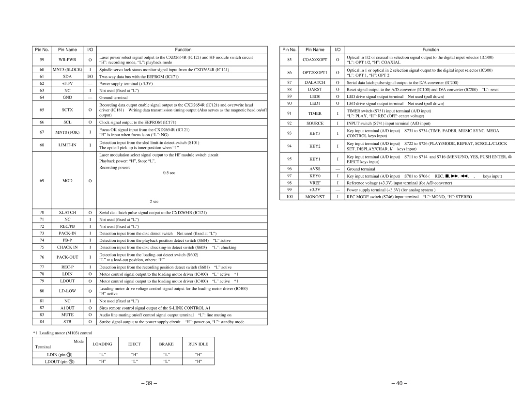
Pin No. | Pin Name | I/O |
|
| Function |
|
|
|
|
|
|
|
| ||
59 |
| O | Laser power select signal output to the CXD2654R (IC121) and HF module switch circuit | ||||
“H”: recording mode, “L”: playback mode |
|
| |||||
|
|
|
|
| |||
|
|
|
|
|
|
| |
60 | MNT3 (SLOCK) | I | Spindle servo lock status monitor signal input from the CXD2654R (IC121) |
| |||
|
|
|
|
|
|
|
|
61 | SDA | I/O |
|
| |||
|
|
|
|
|
|
|
|
62 | +3.3V | — | Power supply terminal (+3.3V) |
|
| ||
|
|
|
|
|
|
|
|
63 | NC | I | Not used (fixed at “L”) |
|
| ||
|
|
|
|
|
|
|
|
64 | GND | — | Ground terminal |
|
| ||
|
|
|
|
|
| ||
|
|
| Recording data output enable signal output to the CXD2654R (IC121) and overwrite head | ||||
65 | SCTX | O | driver (IC181) Writing data transmission timing output (Also serves as the magnetic head on/off | ||||
|
|
| output) |
|
| ||
|
|
|
|
|
|
|
|
66 | SCL | O | Clock signal output to the EEPROM (IC171) |
|
| ||
|
|
|
|
|
|
|
|
67 | MNT0 (FOK) | I | Focus OK signal input from the CXD2654R (IC121) |
|
| ||
“H” is input when focus is on (“L”: NG) |
|
| |||||
|
|
|
|
| |||
|
|
|
|
|
|
|
|
68 | I | Detection input from the sled |
|
| |||
The optical |
|
| |||||
|
|
|
|
| |||
|
|
|
|
|
|
| |
|
|
| Laser modulation select signal output to the HF module switch circuit |
| |||
|
|
| Playback power: “H”, Stop: “L”, |
|
| ||
|
|
| Recording power: |
|
| ||
|
|
|
|
| 0.5 sec |
|
|
69 | MOD | O |
|
|
|
|
|
|
|
|
|
| 2 sec |
|
|
|
|
|
|
|
|
|
|
70 | XLATCH | O | Serial data latch pulse signal output to the CXD2654R (IC121) |
|
| ||
|
|
|
|
|
| ||
71 | NC | I | Not used (fixed at “L”) |
|
| ||
|
|
|
|
|
| ||
72 | REC/PB | I | Not used (fixed at “L”) |
|
| ||
|
|
|
|
| |||
73 | I | Detection input from the disc detect switch Not used (fixed at “L”) |
| ||||
|
|
|
|
|
| ||
74 | I | Detection input from the playback position detect switch (S604) | “L” active |
| |||
|
|
|
|
| |||
75 | CHACK IN | I | Detection input from the disc | “L”: chucking | |||
|
|
|
|
|
| ||
76 | I | Detection input from the |
|
| |||
“L” at a |
|
| |||||
|
|
|
|
| |||
|
|
|
|
|
| ||
77 | I | Detection input from the recording position detect switch (S601) | “L” active |
| |||
|
|
|
|
|
| ||
78 | LDIN | O | Motor control signal output to the loading motor driver (IC400) | “L” active | *1 | ||
|
|
|
|
|
| ||
79 | LDOUT | O | Motor control signal output to the loading motor driver (IC400) | “L” active | *1 | ||
|
|
|
| ||||
80 |
| O | Loading motor drive voltage control signal output for the loading motor driver (IC400) | ||||
“H” active |
|
| |||||
|
|
|
|
| |||
|
|
|
|
|
| ||
81 | NC | I | Not used (fixed at “L”) |
|
| ||
|
|
|
|
|
| ||
82 | A1OUT | O | Sircs remote control signal output of the |
|
| ||
|
|
|
|
| |||
83 | MUTE | O | Audio line muting on/off control signal output terminal “L”: line muting on |
| |||
|
|
|
| ||||
84 | STB | O | Strobe signal output to the power supply circuit “H”: power on, “L”: standby mode | ||||
|
|
|
|
|
|
|
|
*1 Loading motor (M103) control
|
| Mode | LOADING | EJECT | BRAKE | RUN IDLE |
| ||||||
| Terminal | |||||
|
|
|
|
| ||
|
|
|
|
|
|
|
|
| LDIN (pin &¥) | “L” | “H” | “L” | “H” |
|
|
|
|
|
|
|
|
| LDOUT (pin &») | “H” | “L” | “L” | “H” |
|
|
|
|
|
|
|
Pin No. | Pin Name | I/O |
| Function | ||
|
|
|
|
|
| |
85 | COAX/XOPT | O | Optical in 1/2 or coaxial in selection signal output to the digital input selector (IC300) | |||
“L”: OPT 1/2, “H”: COAXIAL |
| |||||
|
|
|
|
|
| |
|
|
|
|
|
| |
86 | OPT2/XOPT1 | O | Optical in 1 or optical in 2 selection signal output to the digital input selector (IC300) | |||
“L”: OPT 1, “H”: OPT 2 |
| |||||
|
|
|
|
|
| |
|
|
|
|
|
| |
87 | DALATCH | O | Serial data latch pulse signal output to the D/A converter (IC200) | |||
|
|
|
|
|
| |
88 |
| DARST | O | Reset signal output to the A/D converter (IC100) and D/A converter (IC200) “L”: reset | ||
|
|
|
|
|
|
|
89 |
| LED0 | O | LED drive signal output terminal | Not used (pull down) | |
|
|
|
|
|
| |
90 |
| LED1 | O | LED drive signal output terminal | Not used (pull down) | |
|
|
|
|
|
| |
91 |
| TIMER | I | TIMER switch (S751) input terminal (A/D input) | ||
| “L”: PLAY, “H”: REC (OFF: center voltage) | |||||
|
|
|
|
| ||
|
|
|
| |||
92 | SOURCE | I | INPUT switch (S741) input terminal (A/D input) | |||
|
|
|
|
|
|
|
93 |
| KEY3 | I | Key input terminal (A/D input) | S731 to S734 (TIME, FADER, MUSIC SYNC, MEGA | |
| CONTROL keys input) |
| ||||
|
|
|
|
|
| |
|
|
|
|
|
|
|
94 |
| KEY2 | I | Key input terminal (A/D input) | S722 to S726 (PLAY/MODE, REPEAT, SCROLL/CLOCK | |
| SET, DISPLAY/CHAR, I/u keys input) | |||||
|
|
|
|
| ||
|
|
|
|
|
|
|
95 |
| KEY1 | I | Key input terminal (A/D input) | S711 to S714 and S716 (MENU/NO, YES, PUSH ENTER, ¤ | |
| EJECT keys input) |
| ||||
|
|
|
|
|
| |
|
|
|
|
|
| |
96 |
| AVSS | — | Ground terminal |
| |
|
|
|
|
|
| |
97 |
| KEY0 | I | Key input terminal (A/D input) | S701 to S706 (r REC, p, ), 0, P, á keys input) | |
98 |
| VREF | I | Reference voltage (+3.3V) input terminal (for A/D converter) | ||
|
|
|
|
| ||
99 |
| +3.3V | — | Power supply terminal (+3.3V) (for analog system ) | ||
|
|
|
| |||
100 | MONO/ST | I | REC MODE switch (S746) input terminal “L”: MONO, “H”: STEREO | |||
|
|
|
|
|
|
|
– 39 – | – 40 – |