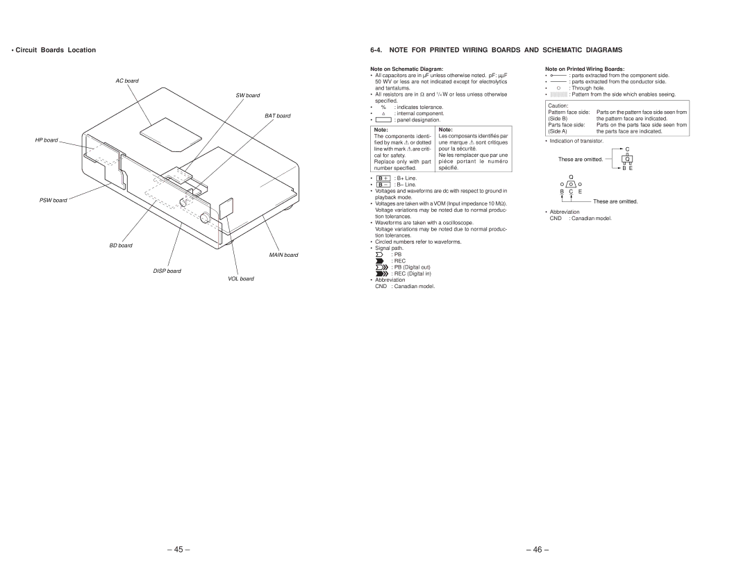
• Circuit Boards Location
AC board
SW board
BAT board
HP board
PSW board
BD board
MAIN board
DISP board
VOL board
Note on Schematic Diagram:
•All capacitors are in µF unless otherwise noted. pF: µµF 50 WV or less are not indicated except for electrolytics and tantalums.
•All resistors are in Ω and 1/4 W or less unless otherwise specified.
•% : indicates tolerance.
•¢ : internal component.
•C : panel designation.
Note: | Note: |
The components identi- | Les composants identifiés par |
fied by mark !or dotted | une marque !sont critiques |
line with mark !are criti- | pour la sécurité. |
cal for safety. | Ne les remplacer que par une |
Replace only with part | piéce portant le numéro |
number specified. | spécifié. |
|
|
•U : B+ Line.
•V : B– Line.
•Voltages and waveforms are dc with respect to ground in playback mode.
•Voltages are taken with a VOM (Input impedance 10 MΩ). Voltage variations may be noted due to normal produc- tion tolerances.
•Waveforms are taken with a oscilloscope.
Voltage variations may be noted due to normal produc- tion tolerances.
•Circled numbers refer to waveforms.
•Signal path. E : PB j : REC
p : PB (Digital out)
l : REC (Digital in)
•Abbreviation
CND : Canadian model.
Note on Printed Wiring Boards:
•X : parts extracted from the component side.
•Y : parts extracted from the conductor side.
•¨ : Through hole.
•b : Pattern from the side which enables seeing.
Caution: |
|
Pattern face side: | Parts on the pattern face side seen from |
(Side B) | the pattern face are indicated. |
Parts face side: | Parts on the parts face side seen from |
(Side A) | the parts face are indicated. |
• Indication of transistor. |
|
|
|
|
|
|
|
|
|
| ||
|
|
|
|
|
| C | ||||||
|
|
|
|
|
|
|
|
|
|
|
|
|
These are omitted. |
|
|
|
|
| Q | ||||||
|
|
|
| |||||||||
![]() B E
B E
Q
B C E
These are omitted.
• Abbreviation
CND : Canadian model.
– 45 – | – 46 – |