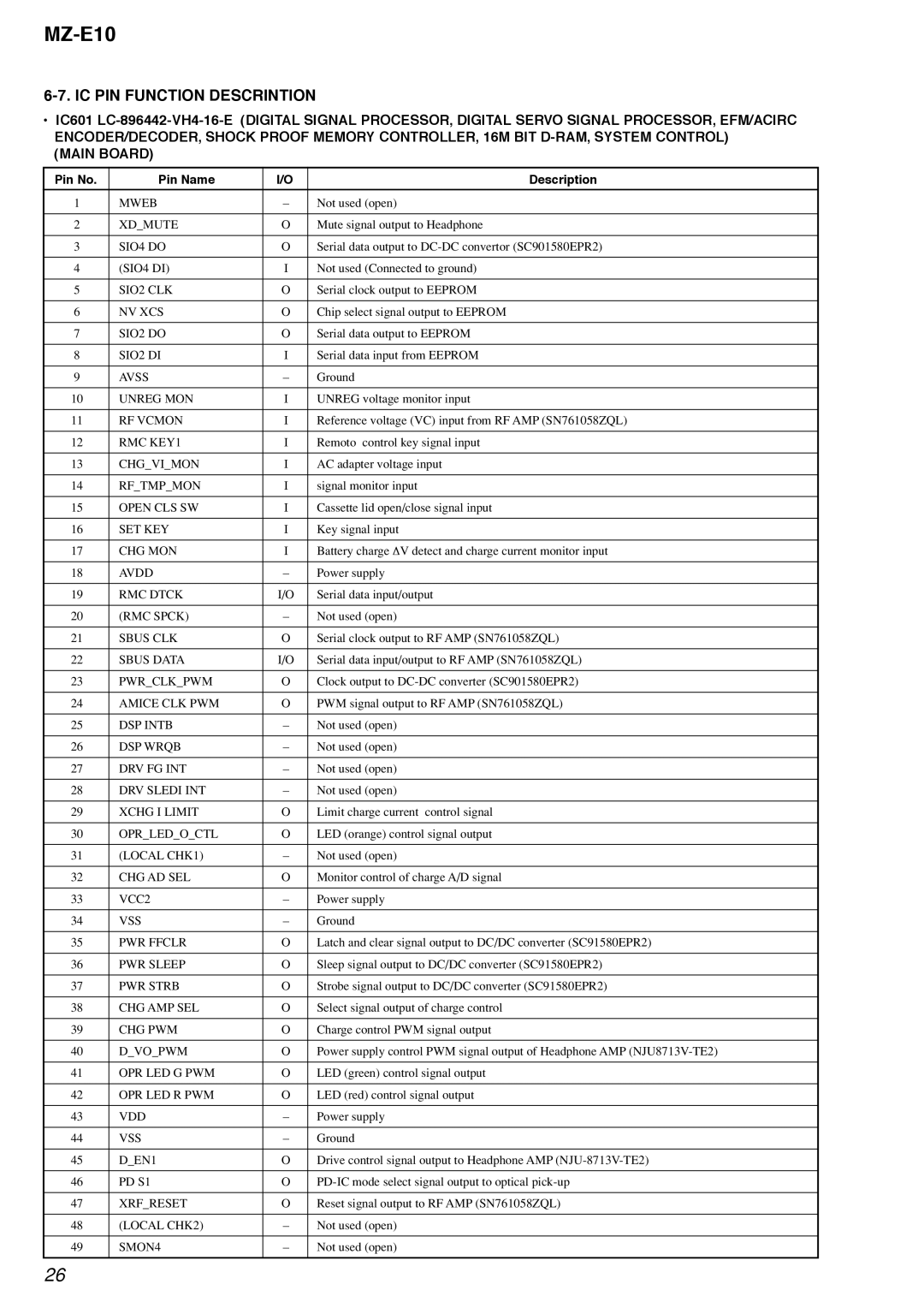
MZ-E10 specifications
The Sony MZ-E10, a compact MiniDisc player released during the height of the MiniDisc era, is renowned for its portability and impressive features tailored for audiophiles and casual listeners alike. Designed with user-friendliness in mind, the MZ-E10 weighs just 130 grams and fits easily into pockets or bags, making it the ideal companion for music on the go.One of the standout features of the Sony MZ-E10 is its ability to record audio digitally, allowing users to contribute their own music to the MiniDisc format. This recording feature utilizes Sony's advanced ATRAC (Adaptive Transform Acoustic Coding) algorithm, which compresses audio without a significant loss in quality. This means that listeners can enjoy high-quality sound while optimizing storage space on their MiniDiscs.
The MZ-E10 supports various playback modes, including standard play and shuffle, enhancing the listening experience. Moreover, it boasts an easy-to-read LCD display that shows track information, battery life, and various playback settings. The user interface is straightforward, featuring tactile buttons that facilitate navigating through menus and playlists.
Battery life is another key characteristic, as the MZ-E10 can offer extended playback times with just a single AA battery. This efficiency is perfect for users who may be traveling or away from power sources for extended periods. To further enhance its functionality, the player features a line-in recording capability, allowing connection to external devices for capturing audio, such as recordings from vinyl or cassettes.
In terms of design, the MZ-E10 exudes a sleek and modern aesthetic, with a durable casing designed to withstand the rigors of daily use. The player is equipped with a headphone jack that supports both standard and high-impedance headphones, catering to a variety of audio preferences.
Overall, the Sony MZ-E10 stands as a testament to innovative technology in portable music playback. With its combination of compact design, high-quality audio recording and playback, and user-friendly features, it secured its place in the hearts of many music enthusiasts during its time. While modern technology has shifted primarily towards digital streaming and solid-state formats, the MZ-E10 remains a cherished artifact for those who appreciate the unique qualities of the MiniDisc system.
